Scanning electron microscope

a scanning electron microscope and microscope technology, applied in the field of scanning electron microscopes, can solve the problems of reducing measurement precision, insufficient measurement precision, and inability to obtain clear images with sufficient measurement precision, and achieve the effect of measuring precision

Active Publication Date: 2011-10-13
HITACHI HIGH-TECH CORP
View PDF0 Cites 14 Cited by
  • Summary
  • Abstract
  • Description
  • Claims
  • Application Information

AI Technical Summary

Benefits of technology

[0010]Clear images can be obtained even at high magnification. Specifically, the image drift rate (shift rate) of field images included in a frame image, and the field images are corrected, thereafter accumulating the field images so as to form a frame image. Based on the obtained image, the pattern dimensions on the semiconductor substrate or insulating substrate are obtained. Thus, the measurement precision can sufficiently be achieved even with fine patterns.

Problems solved by technology

This causes a problem such as image blur, resulting in a decrease in measurement precision.
However, according to the technique for correcting the image shift rate between the images (frame images) disclosed in Japanese Patent Application Laid-Open Publication No. 2006-308471, it is found that clear images cannot sufficiently be obtained with sufficient measurement precision, due to the occurrence of an image blur at high magnification (particularly, it is remarkable at or below approximately 1 micron of the observation field).

Method used


Image

  • Scanning electron microscope
  • Scanning electron microscope
  • Scanning electron microscope

Examples


first embodiment

[0025]The first embodiment of the present invention will now be described with reference to the drawings.

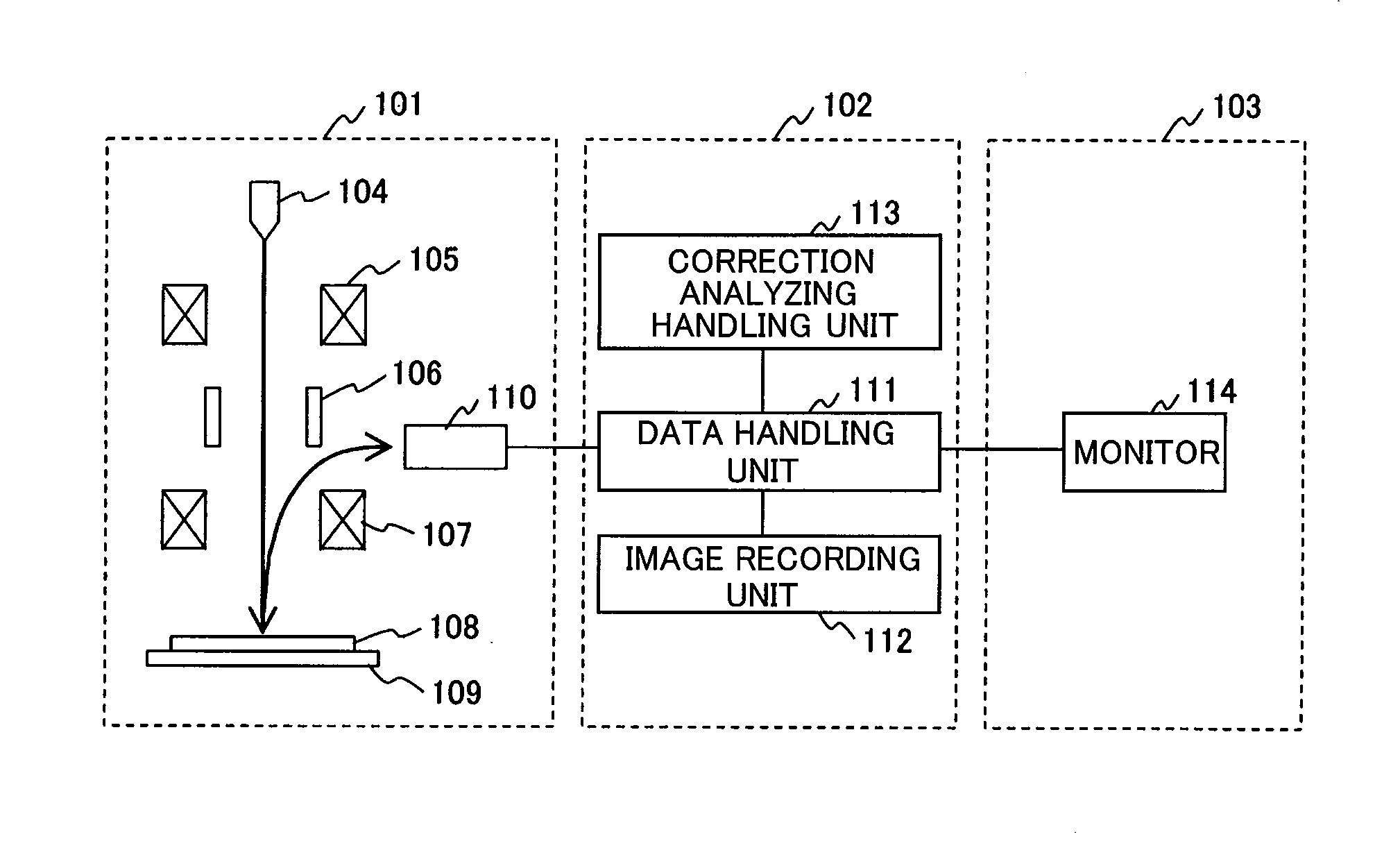
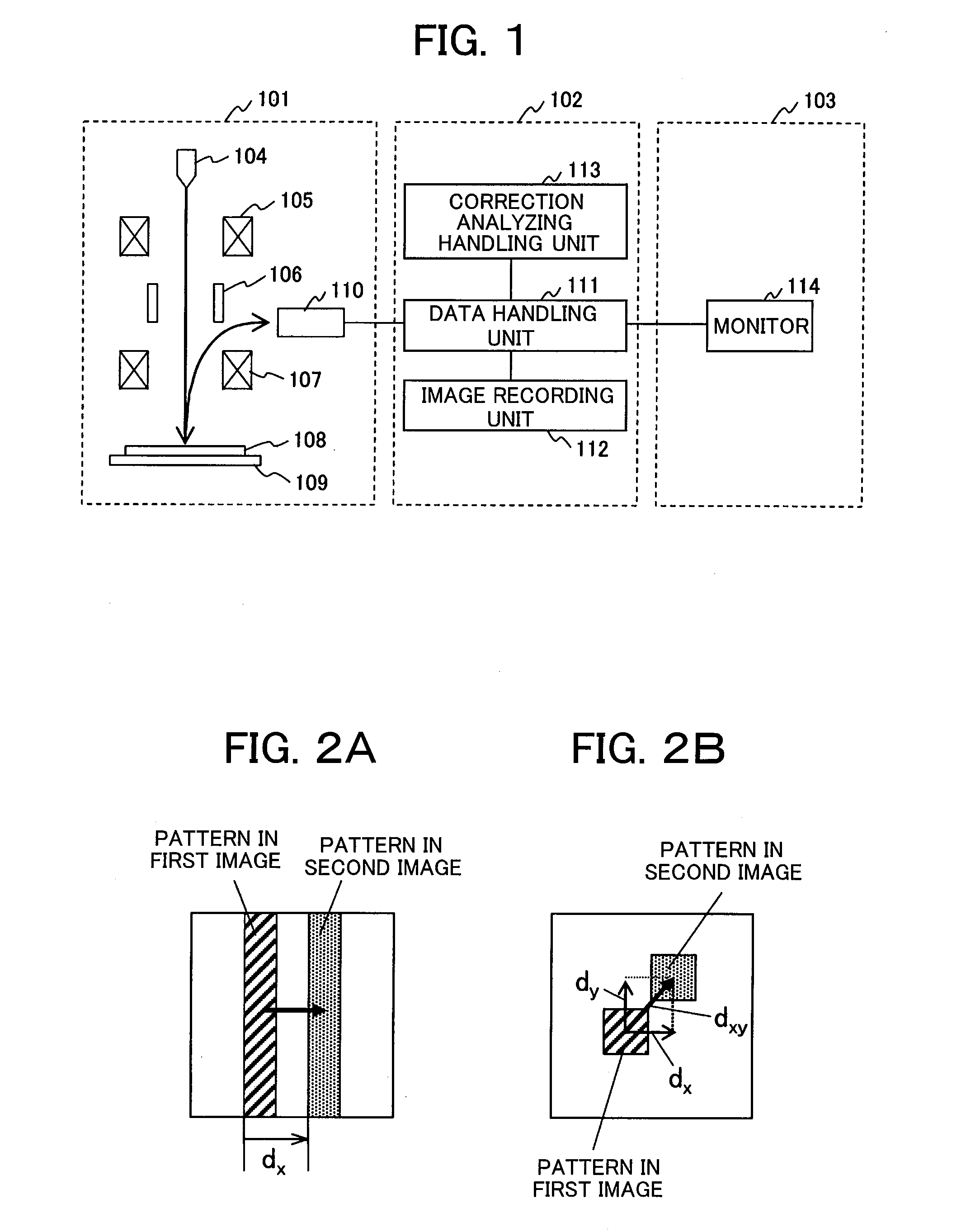
[0026]FIG. 1 shows an embodiment of a scanning electron microscope including a drift correction function. This apparatus makes it possible to acquire clear frame images by calculating a drift rate and correcting drift, even if the image drift occurs. The image drift is a phenomenon that the images shift with time at observation of a sample. In this description, the “drift rate” implies the amount of positional deviation (shift rate) of patterns between frame images shown in FIG. 2 and also the shift rate between field images.

[0027]The scanning electron microscope including an image correction function includes an electron microscope unit 101, a control unit 102, and a display unit 103. An electron beam emitted from an electron source 104 is focused by a condenser lens 105 and an objective lens 107, then irradiated onto a sample 108. The electron beam is scanned two-dimensionally ...

second embodiment

[0057]Descriptions will now be made of the second embodiment using FIG. 10 and FIG. 11. The contents of the first embodiment are applicable also to this embodiment, unless special circumstances are present.

[0058]FIG. 10 is a flowchart showing the process of this embodiment. Descriptions will now be made of this flowchart.

[0059]The stage is moved to an observation point. Then, plural one-frame images are continuously acquired in the same field. The frame images thus acquired are stored in the image recording unit 112 (S1001).

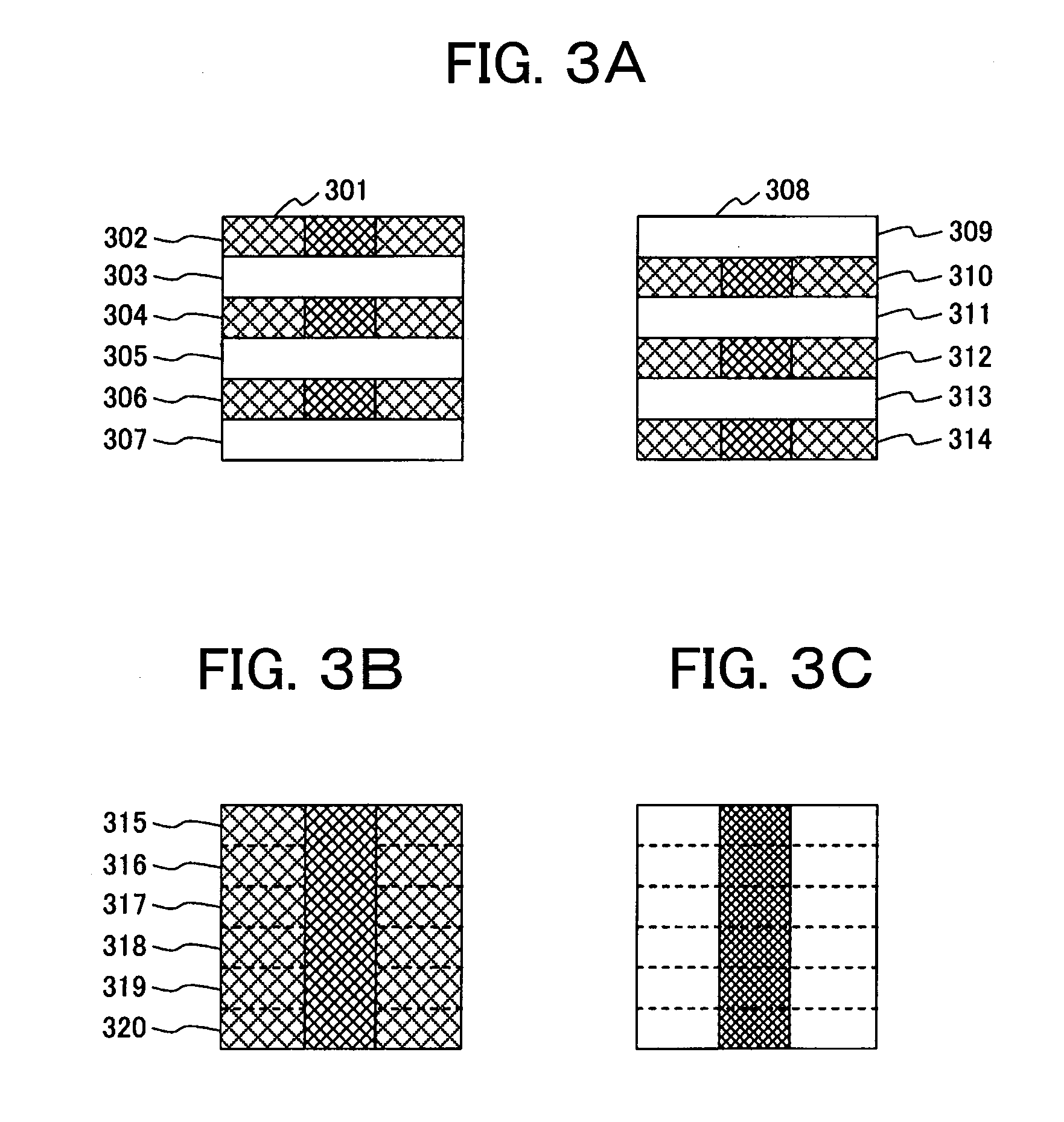
[0060]The correction analyzing handling unit 113 is used for reducing the frame images so as to improve the S / N ratio (S1002).

[0061]The correction analyzing handling unit 113 is used for judging whether the pattern is one-dimensional or two-dimensional, using Computer Aided Design (CAD) data as design data corresponding to the target pattern to be observed or frame image data which has been acquired through the observation. In addition, an applicable analyzing me...

third embodiment

[0072]Descriptions will now be made of the third embodiment of the present invention. The contents of the first embodiment are applicable also to this embodiment, unless special circumstances are present.

[0073]In the first embodiment, the drift rate of each frame has been obtained, and the obtained drift rate is divided into the number of field images, so as to perform drift correction. In this technique, the calculation of the drift rate is made by comparing the one-frame images. However, the drift rate cannot be obtained with high accuracy between the one-frame images as they are when the S / N ratio is remarkably low. In consideration of this, according to one technique, correction is performed by superimposing plural one-frame images so as to form a new image, and obtaining a drift rate between these images with an improved S / N ratio. The minimum number of one-frame images to be superimposed is set so that an S / N ratio capable of obtaining the drift rate is obtained. In this case,...


PUM


Abstract

Provided is a scanning electron microscope including: an image recording unit (112) which stores a plurality of acquired frame images; a correction analyzing handling unit (113) which calculates a drift amount between frame images and a drift amount between a plurality of field images constituting a frame image; and a data handling unit (111) which corrects positions of respective field images constituting the plurality of fields images according to the drift amount between the field images and superimposes the field images on one another so as to create a new frame image. This provides a scanning electron microscope which can obtain a clear frame image even if an image drift is caused during observation of a pattern on a semiconductor substrate or an insulating object.

Description

FIELD OF THE INVENTION[0001]The present invention relates to a scanning electron microscope, and, more particularly, to a scanning electron microscope suitable for observing images at high magnification.DESCRIPTION OF THE RELATED ART[0002]Those scanning electron microscopes are systems for forming images. Specifically, a sample is irradiated with an electron beam which has been finely narrowed, and a secondary electron and a backscattered electron generated by the irradiation of the electron beam are detected. Based on the detection amount, the contrast is modulated, thereby forming images (see Japanese Patent Application Laid-Open Publication No. 2006-308471).SUMMARY OF THE INVENTION[0003]In recent years, the pattern dimensions formed on a semiconductor substrate or insulating substrate are made more and more finely. Thus, it is required that the observation and critical dimension measurement should be done at high magnification, using the scanning electron microscope.[0004]When a ...

Claims


Application Information

Patent Timeline
Patent Type & Authority Applications(United States)
IPC IPC(8): H04N7/18
CPCG01B15/00H01J37/28H01J37/222
Inventor OKAI, NOBUHIROSOHDA, YASUNARI
Owner HITACHI HIGH-TECH CORP
Why Eureka
Try Eureka