

Flip-Flop and Frequency Dividing Circuit with Flip-Flop
- Summary
- Abstract
- Description
- Claims
- Application Information
AI Technical Summary
Benefits of technology
Problems solved by technology
Method used
Image

Examples
Embodiment Construction
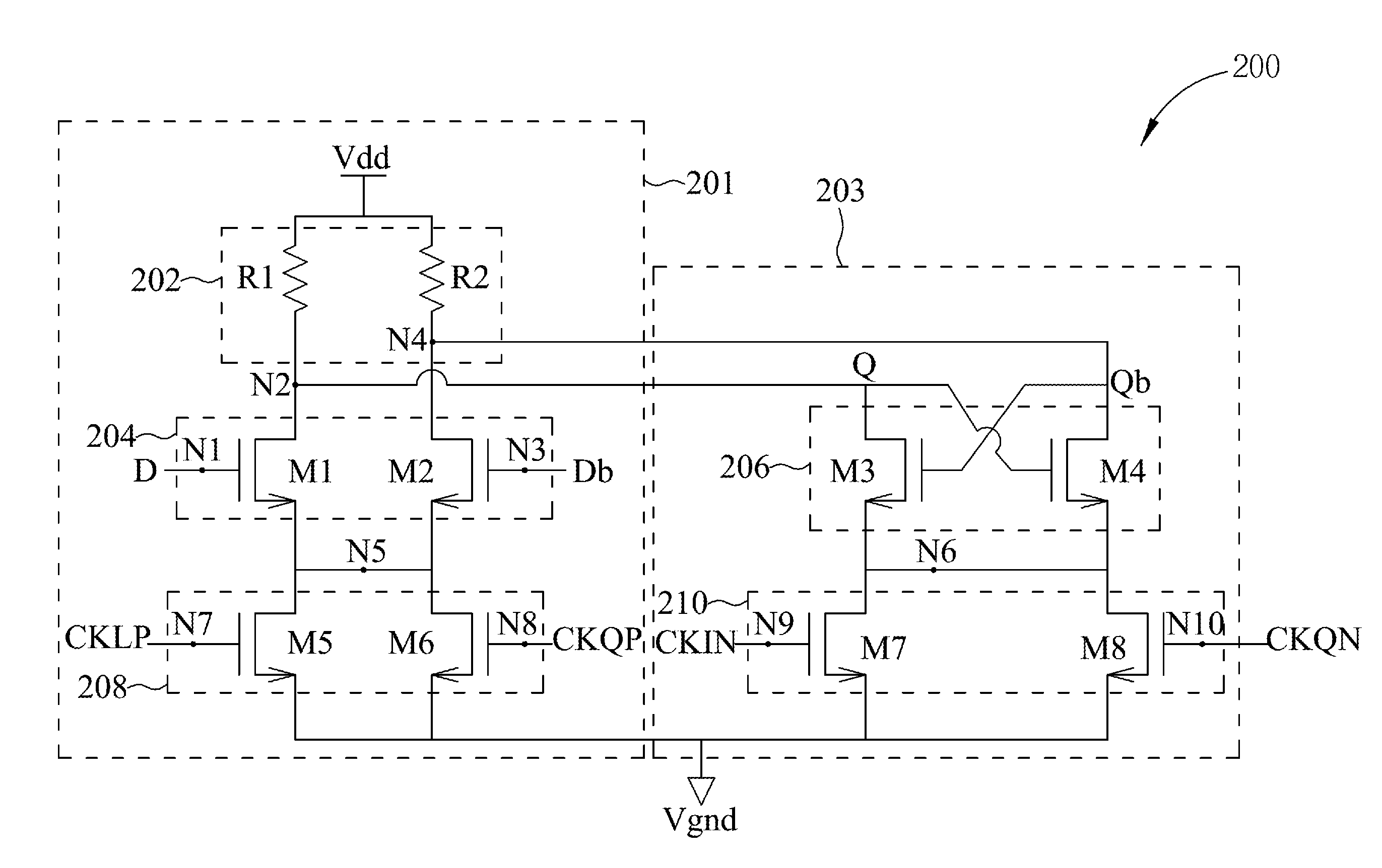
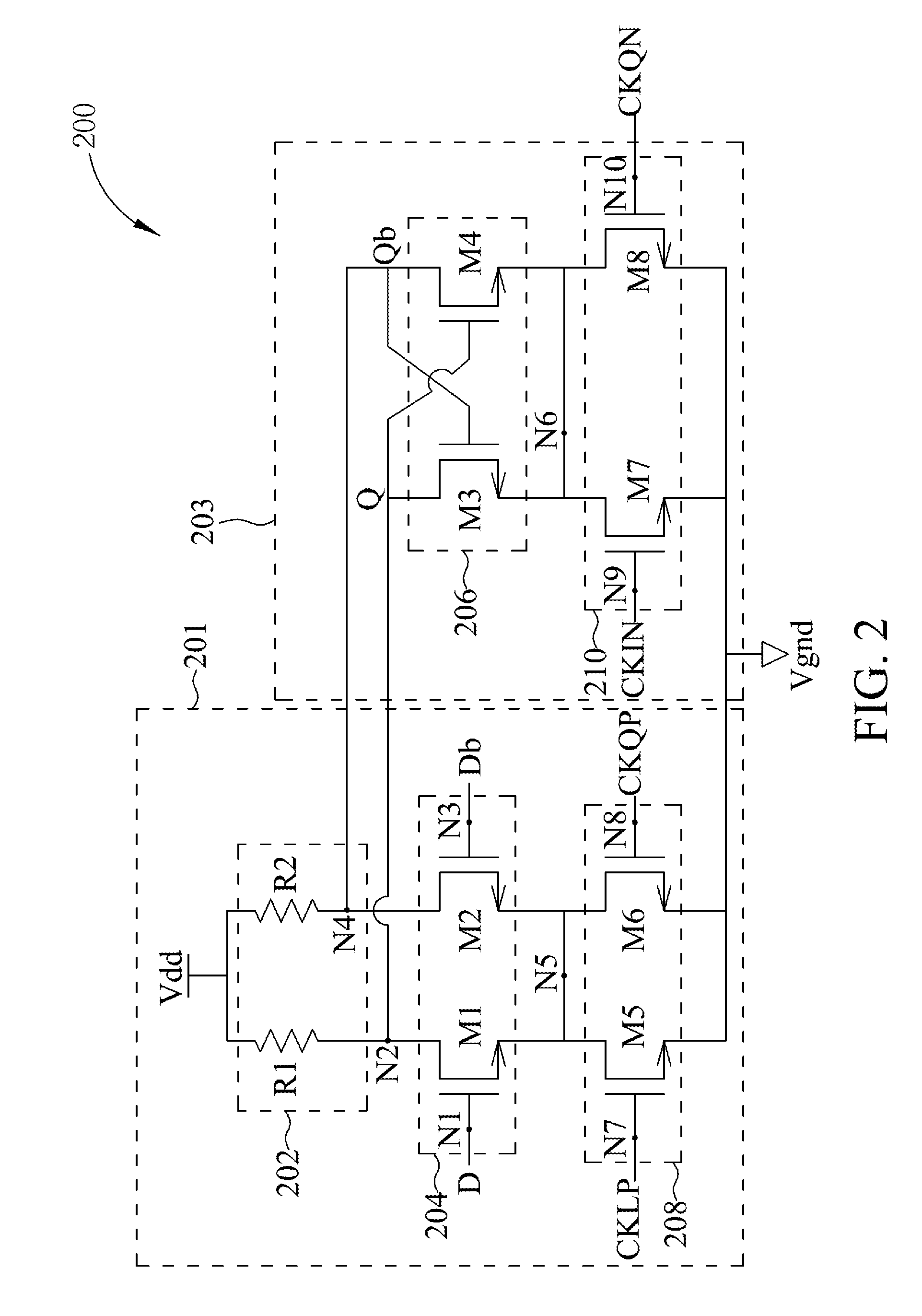
[0012]FIG. 2 is a schematic diagram of a flip-flop 200 in accordance with an embodiment of the present disclosure. The flip-flop 200 comprises an input stage 201 and a latch stage 203. The input stage 201 comprises a load 202, a signal input circuit 204 and a first control circuit 208. The latch stage 203 comprises a cross-coupled pair circuit 206 and a second control circuit 210. The load 202 is coupled to a first voltage level Vdd that is a power supply voltage. The signal input circuit 204 serially connected to the load 202 receives input signal D and Db. In this embodiment, the input signal is a differential pair. The cross-coupled pair circuit 206 coupled to a connection node of the load 202 and the signal input circuit 204 generates a differential pair of output signals Q and Qb. The first control circuit 208 coupled between the signal input circuit 204 and a second voltage level Vgnd receives a first clock signal CKIP and a second clock signal CKQP, and the second voltage lev...
PUM
 Abstract
Description
Claims
Application Information