Cell with surrounding word line structures and manufacturing method thereof

a cell and word technology, applied in the direction of transistors, electrical devices, semiconductor devices, etc., can solve the problem of limited size of one bit lines, and achieve the effect of increasing the speed of the transistor

Inactive Publication Date: 2011-10-27
INOTERA MEMORIES INC
View PDF3 Cites 4 Cited by
  • Summary
  • Abstract
  • Description
  • Claims
  • Application Information

AI Technical Summary

Benefits of technology

[0007]The objective of the present invention is to provide a memory cell characterized in surrounding word line structures that the speed of the transistor can be increased.
[0012]Step 4: forming a plurality of transistors in the active area; wherein each the transistor is controlled by two gates defined of the two word lines and one of the bit lines for increasing switching rates.
[0014]The present invention further provides a cell with surrounding word line structures, comprising: an active area; a plurality of first trenches formed in the active area and extending in a first direction; wherein each the first trench has a bit line on a side thereof; a plurality of second trenches formed in the active area and extending in a second direction; wherein each the second trench has two word lines respectively formed on two sides of the second trench; and a plurality of transistors formed in the active area; wherein each the transistor is controlled by the bit line and the two word lines, the word lines are constructed to the surrounding word line structures, and each the transistor is controlled by two gates defined of the two word lines for increasing switching rates.
[0015]The transistor of the present invention is controlled by two word lines and one bit line. The single bit line having lower resistance and the two channels defined by the two word lines result in the higher speed of the memory cell.

Problems solved by technology

In the traditional cell structure, bit lines are formed on both sides of the trench; therefore, the size of one bit line is limited.

Method used


Image

  • Cell with surrounding word line structures and manufacturing method thereof
  • Cell with surrounding word line structures and manufacturing method thereof
  • Cell with surrounding word line structures and manufacturing method thereof

Examples


Embodiment Construction

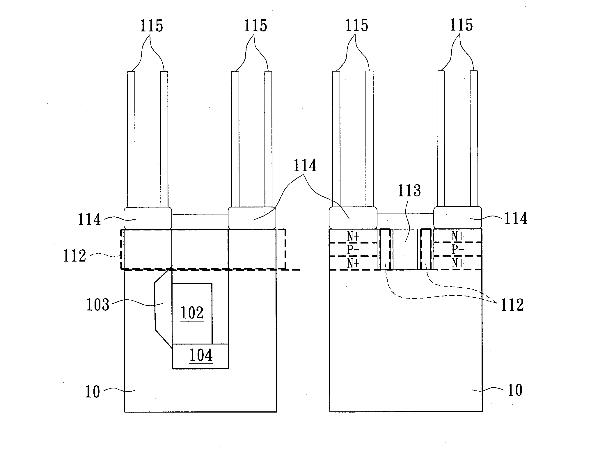
[0024]The present invention provides a memory cell having surrounding word line structures and a manufacturing method thereof. The memory cell has two gates (i.e., word lines) on two sides of a transistor. The gates define a pair of channel that can increase the switching rate of the transistor. Furthermore, the transistor is controlled by a single bit line having a lager size than the traditional bit line pair. Therefore, the digital line defined by the larger bit line of the present invention has an improved transfer rate.

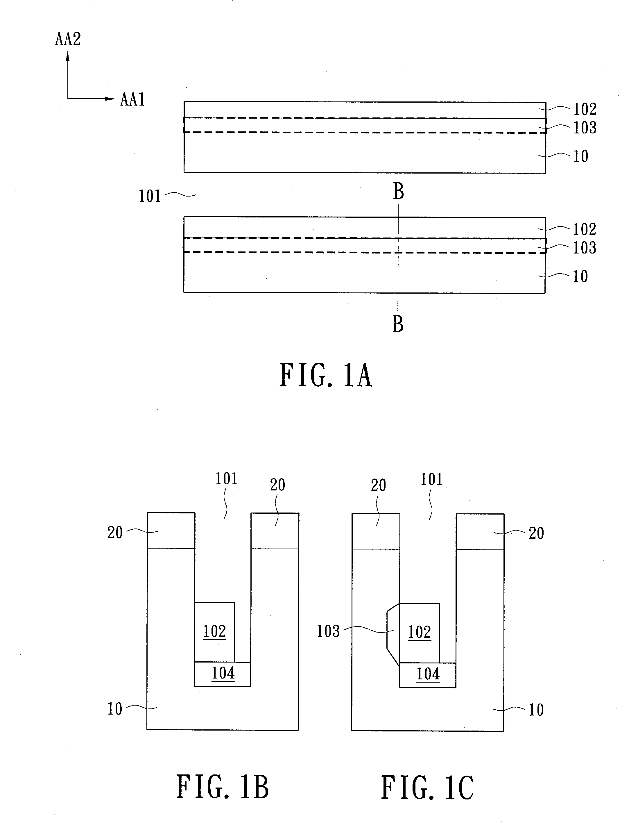
[0025]Please refer to FIGS. 1A to 7B. The method of manufacturing the memory cell according to the instant disclosure is discussed as follows.

[0026]First, providing an active area 10 and forming a plurality of first trenches 101 along a first direction on the active area 10. As shown in FIG. 1A, the direction AA1 is chosen to be the first direction. Next, forming a bit line 102 on a sidewall in the first trench 101. Comparing to the traditional structure where a ...


PUM


Abstract

A memory cell with surrounding word line structures includes an active area; a plurality of first trenches formed on the active area in a first direction, each first trench has a bit line on a sidewall therein; a plurality of second trenches formed on the active area in a second direction, each second trench has two word lines formed correspondingly on the sidewalls in the second trench; and a plurality of transistors formed on the active area. The word line pairs are arranged into a surrounding word line structure. The transistor is controlled by the bit line and the two word lines, thus improving the speed of the transistor.

Description

BACKGROUND OF THE INVENTION[0001]1. Field of the Invention[0002]The present invention is a cell with surrounding word line structures and the manufacturing method thereof; especially, the present invention relates to cell having improved speed and the manufacturing method thereof.[0003]2. Description of Related Art[0004]The memory cells of DRAM usually have FET devices and capacitors. In other words, the cell is consisted of a capacitor and a transistor for controlling the charging / discharging and reading. The transistor is controlled by word lines and bit lines. It plays an important role for improving the on / off speed of the transistor.[0005]In the traditional cell structure, bit lines are formed on both sides of the trench; therefore, the size of one bit line is limited. The smaller bit line results in the higher resistance and further in the lower speed. On the other hand, only a word line is formed to control the on / off of the transistor. Therefore, the switching rate of the tr...

Claims


Application Information

Patent Timeline
Patent Type & Authority Applications(United States)
IPC IPC(8): H01L27/108H01L21/8242
CPCH01L21/26586H01L27/10876H01L29/7827H01L29/66666H01L27/10891H10B12/053H10B12/488
Inventor LEE, TZUNG HANHUANG, CHUNG-LINLIU, HSIEN-WEN
Owner INOTERA MEMORIES INC
Why Eureka
Try Eureka