Spin Transfer Torque Memory Device Having Common Source Line and Method for Manufacturing the Same

a technology of spin transfer torque and memory device, which is applied in the direction of semiconductor devices, electrical appliances, basic electric elements, etc., can solve the problems of reducing the signal the resistance of the source line becomes larger, and the speed of flash memory is slower than that of the dram, so as to improve the spin transfer torque memory, reduce the resistance of the source line, and improve the effect of spin transfer torque memory

Inactive Publication Date: 2011-11-03
SK HYNIX INC
View PDF0 Cites 56 Cited by
  • Summary
  • Abstract
  • Description
  • Claims
  • Application Information

AI Technical Summary

Benefits of technology

[0022]Various embodiments of the invention are directed at providing an improved spin transfer torque memory device, thereby reducing resistance of a source line for high integration.

Problems solved by technology

However, the flash memory has a slower speed and a higher operating voltage than that of the DRAM.
However, in this case, since the critical dimension of a buried bit line (BBL) used as a source line is narrow, the resistance of the source line becomes larger.
When the data of the MTJ is read, its signal is degraded, and the size of current required in the write mode is limited.

Method used


Image

  • Spin Transfer Torque Memory Device Having Common Source Line and Method for Manufacturing the Same
  • Spin Transfer Torque Memory Device Having Common Source Line and Method for Manufacturing the Same
  • Spin Transfer Torque Memory Device Having Common Source Line and Method for Manufacturing the Same

Examples


Embodiment Construction

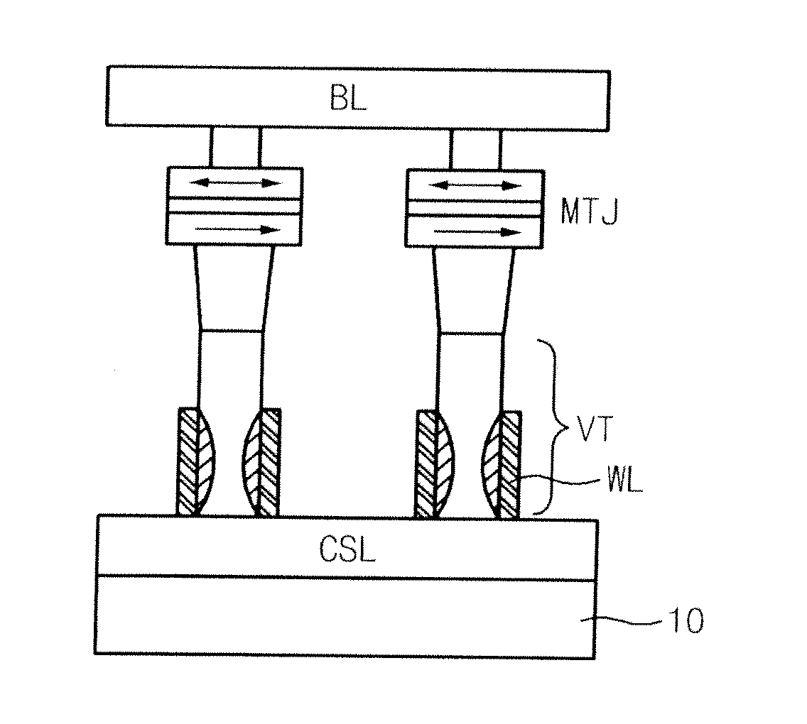
[0037]FIG. 3 is a diagram illustrating a spin transfer torque memory device according to an embodiment of the invention.

[0038]The spin transfer torque memory device of FIG. 3 comprises a common source line (CSL), a vertical transistor (VT), a Magnetic Tunnel Junction (MTJ) and a bit line (BL).

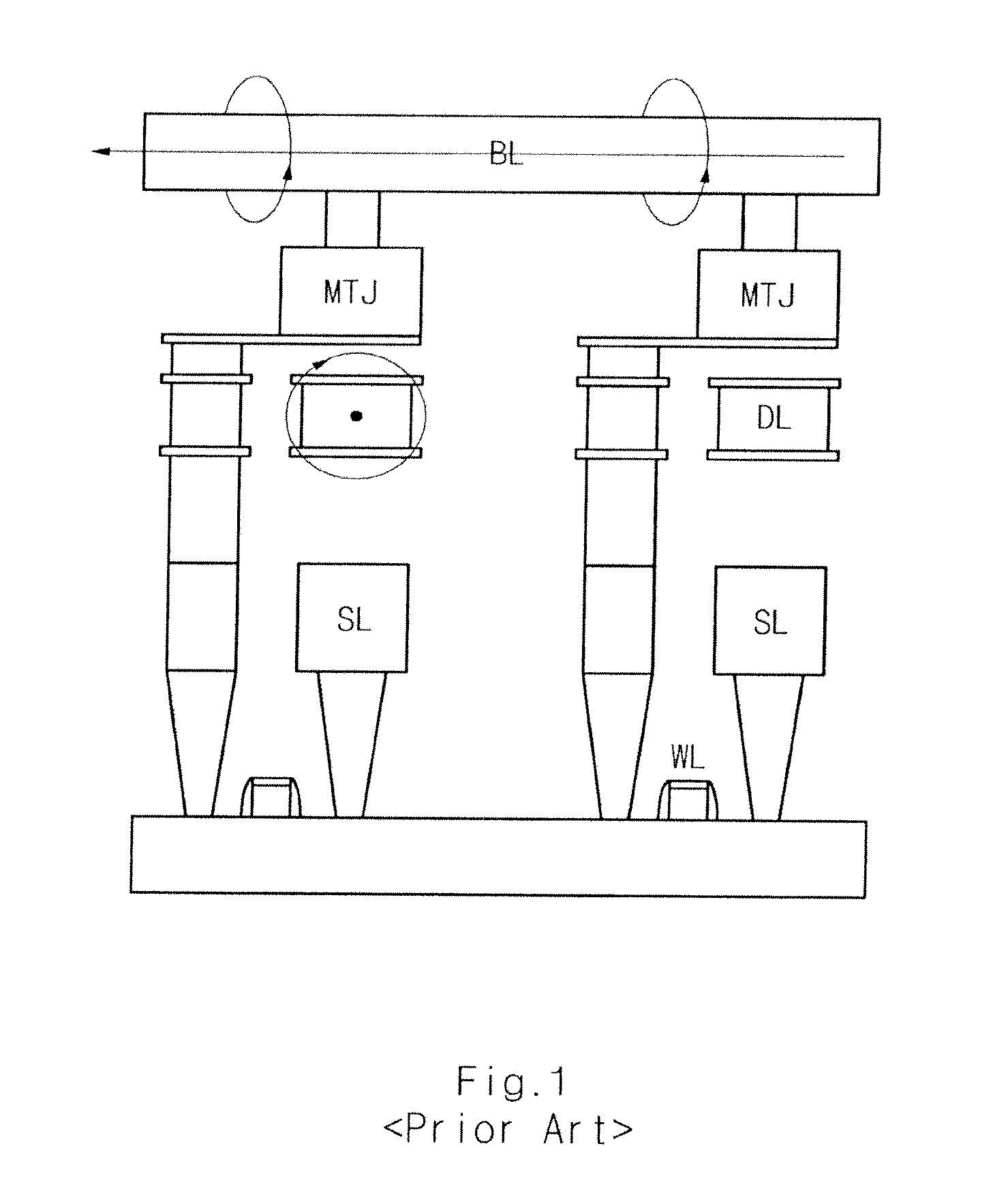
[0039]The CSL formed over a silicon substrate 10 connects source / drain regions of the bottom portion of the VT in common. In order to obtain the CSL, after a pillar for forming the VT is formed, impurities are ion-implanted into the silicon substrate. Otherwise, before the pillar is formed, a metal is deposited over the silicon substrate 10. In this way, the CSL having a large area is formed to connect the source / drain regions of the VT in common in a cell region. As a result, the resistance of the source line can be reduced, and it is not necessary to form an additional selecting circuit (not shown) for selecting the source line during a data write mode in a core region (not shown).

[0040]The V...


PUM


Abstract

A spin transfer torque memory device and a method for manufacturing the same. The spin transfer torque memory device comprises a MRAM cell using a MTJ and a vertical transistor. A common source line is formed in the bottom of the vertical transistor, thereby obtaining the high-integrated and simplified memory device.

Description

[0001]This application is a division of U.S. application Ser. No. 12 / 343,556, filed Dec. 24, 2008, which claims priority to Korean Patent Application No. 10-2008-0088823, filed on Sep. 9, 2008, the disclosures of which are hereby expressly incorporated herein for all purposes.BACKGROUND OF THE INVENTION[0002]The present invention generally relates to a spin transfer torque memory (STT-MRAM), and more specifically, to a STT-MRAM having a common source line and a method for manufacturing the same.[0003]Out of all semiconductor memory devices, DRAM has had the largest market share.[0004]The DRAM that includes one MOS transistor and one capacitor which are paired is a memory device operated as one bit. The DRAM requires a periodic refresh operation in order not to lose data because the DRAM stores charges in the capacitor to write data.[0005]A nonvolatile memory which have stored signals that are not destroyed when a power source turns off such as a hard disk includes NAND / NOR flash mem...

Claims


Application Information

Patent Timeline
Patent Type & Authority Applications(United States)
IPC IPC(8): H01L21/8246
CPCH01L27/228H01L29/7827H01L29/66666H10B61/22H01L29/513H10N70/801
Inventor KIM, HYUN JEONGCHUNG, SUNG WOONG
Owner SK HYNIX INC
Why Eureka
Try Eureka