Printed circuit board and layout method thereof

a technology of printed circuit boards and layout methods, applied in printed circuits, waveguides, instruments, etc., can solve problems such as increased cost, occupied extra space, and digital system failures

Inactive Publication Date: 2011-11-10
HON HAI PRECISION IND CO LTD
View PDF0 Cites 12 Cited by
  • Summary
  • Abstract
  • Description
  • Claims
  • Application Information

AI Technical Summary

Problems solved by technology

Crosstalk can cause digital system failure due to false signals appearing on a receiver.
A typical layout method for reducing the crosstalk is to increase the distance between the two conductors, which occupies extra space and increases the cost.

Method used


Image

  • Printed circuit board and layout method thereof
  • Printed circuit board and layout method thereof
  • Printed circuit board and layout method thereof

Examples


Embodiment Construction

[0014]The disclosure is illustrated by way of example and not by way of limitation in the figures of the accompanying drawings in which like references indicate similar elements. It should be noted that references to “an” or “one” embodiment in this disclosure are not necessarily to the same embodiment, and such references mean at least one.

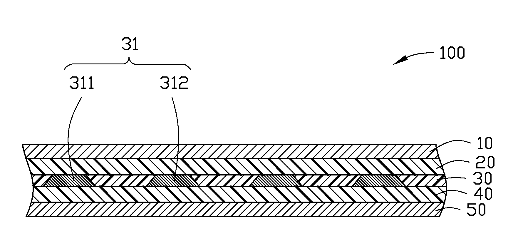
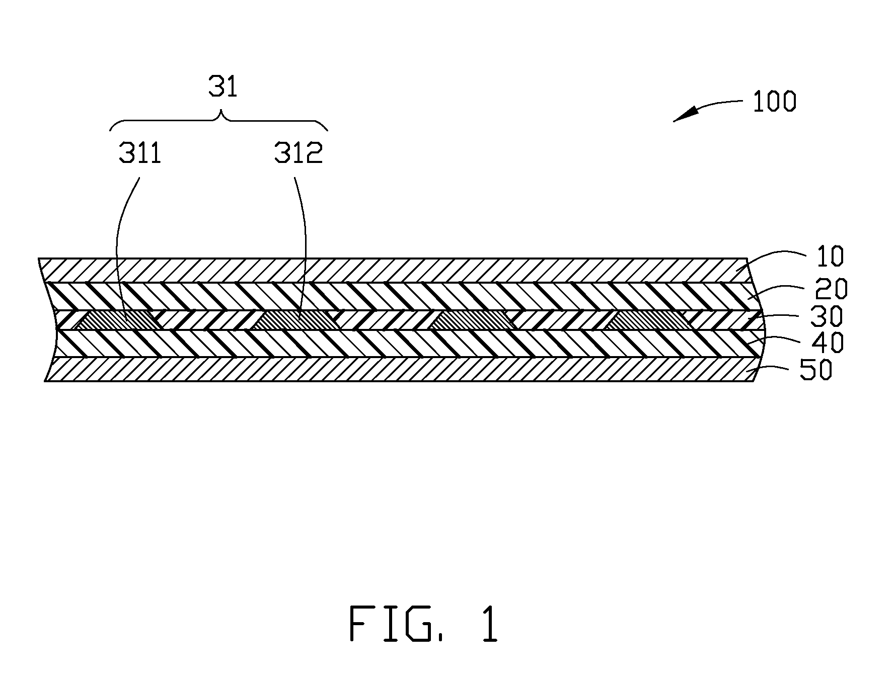
[0015]Referring to FIG. 1, a printed circuit board 100 includes a first reference layer 10, a first dielectric layer 20, a signal layer 30, a second dielectric layer 40 and a second reference layer 50 arrayed in sequence from top to bottom. The signal layer 30 sets at least a pair of differential transmission lines 31 thereon. Each differential transmission line 31 includes a first transmission line 311 and a second transmission line 312 which are strip lines. A plurality of dielectric material is disposed between each adjacent first and second transmission lines 311 and 312. A width of each of the first and second transmission lines 311 and 312 ...


PUM


Abstract

A printed circuit board layout method includes the following steps. A printed circuit board with a signal layer and a pair of differential transmission lines positioned on the signal layer is provided. A first distance is determined; when the distance between the pair of differential transmission lines is greater than the first distance, an eye width and an eye height of an eye diagram nearly remains the same. When a distance between the pair of differential transmission lines is less than the first distance, an eye width and an eye height of an eye diagram decreases. A second distance that is less than the first distance is set between the pair of differential transmission lines which makes the eye width and the eye height greater than a predetermined value, and which is determined by a Far End Crosstalk (FEXT) on the eye diagram when the pair differential transmission lines transmit signals.

Description

BACKGROUND [0001]1. Technical Field[0002]The present disclosure relates to printed circuit boards and specifically to a printed circuit board and a layout method thereof that can save layout space on the printed circuit board.[0003]2. Description of Related Art[0004]Printed circuit boards are designed for coupling control chips and electronic devices, to transmit signals such as high-speed differential signals. Mutual capacitance is the coupling of two electric fields. Similarly, if two conductors are in close proximity with each other, a voltage will be generated in the second conductor as a result. This is mutual inductance.[0005]Crosstalk is the electrical “noise” caused by mutual inductance and mutual capacitance between signal conductors, due to the close proximity of the signal conductors to each other. Crosstalk can cause digital system failure due to false signals appearing on a receiver. A typical layout method for reducing the crosstalk is to increase the distance between ...

Claims


Application Information

Patent Timeline
Patent Type & Authority Applications(United States)
IPC IPC(8): H01P3/08G06F17/50
CPCH05K1/0245
Inventor LIN, YU-HSU
Owner HON HAI PRECISION IND CO LTD
Why Eureka
Try Eureka