Method and system for quickly identifying circuit components in an emission image

a technology of emission image and circuit components, applied in image enhancement, image data processing, instruments, etc., can solve the problems of increasing difficulty in precise localization and interpretation of measured results

Active Publication Date: 2011-11-17
IBM CORP
View PDF8 Cites 19 Cited by
  • Summary
  • Abstract
  • Description
  • Claims
  • Application Information

AI Technical Summary

Benefits of technology

[0008]A system and method for localization and resolvability of an integrated circuit includes electrical stimuli equipment configured to apply a set of stimuli to a device under test such that the electrical stimuli are chosen so that upon a change in a stimulus a different optical effect is provided by measured emissions from the device under test. An emission measurement system is configured to collect emissions from the device under test for each electrical stimuli in the set of stimuli to provide a measurement data set. A data comparison module is configured to analyze the measurement data set to localize and evaluate circuit structures of the device under test.

Problems solved by technology

The continuous trend of modern complementary metal oxide semiconductor (CMOS) VLSI circuits towards miniaturization makes the precise localization and interpretation of the measured results more and more challenging.
Additionally, near field microscopy, with all the complications and limitations associated to it, may lead to increased spatial resolution in static emission measurements for certain localized areas of interest.

Method used


Image

  • Method and system for quickly identifying circuit components in an emission image
  • Method and system for quickly identifying circuit components in an emission image
  • Method and system for quickly identifying circuit components in an emission image

Examples


Embodiment Construction

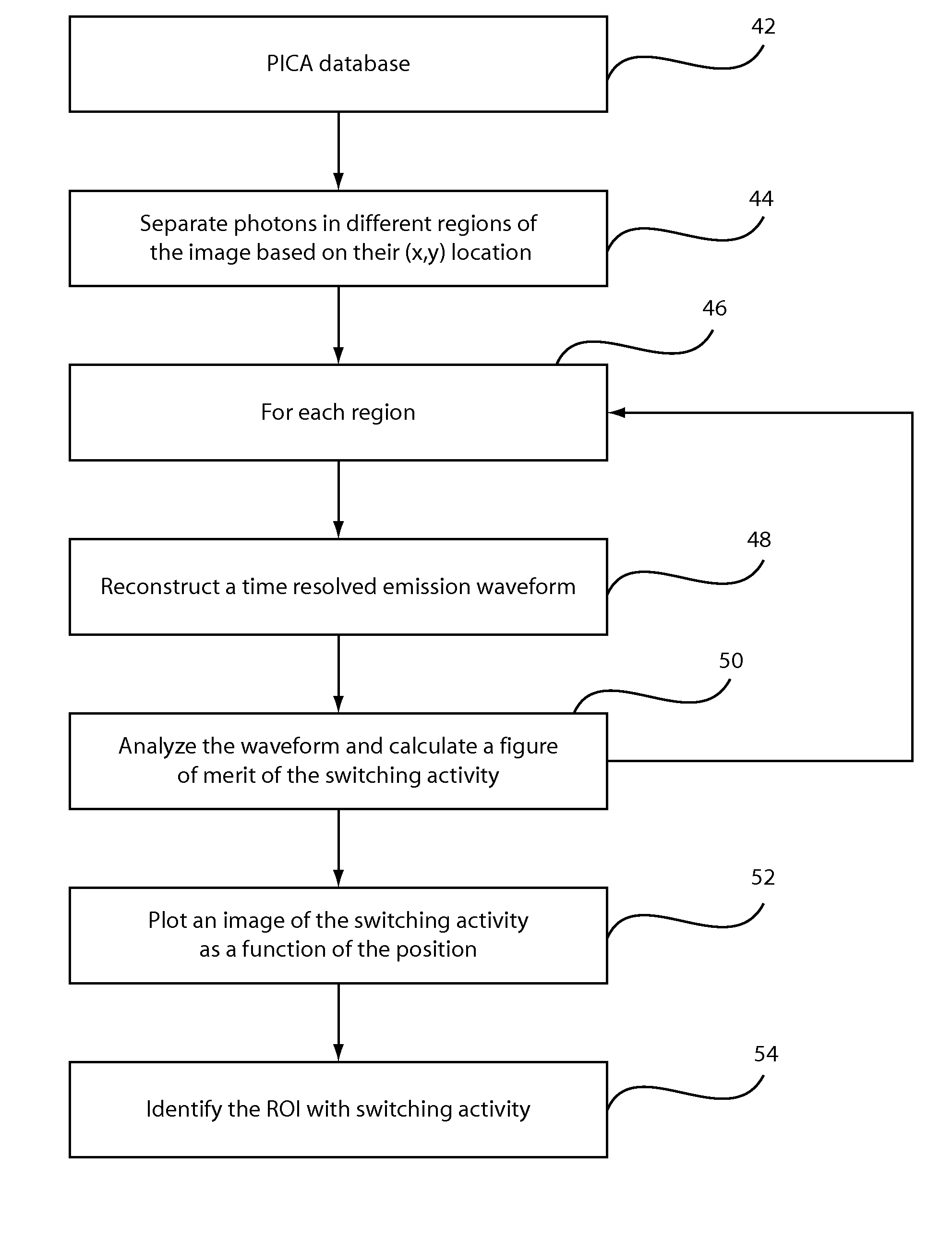
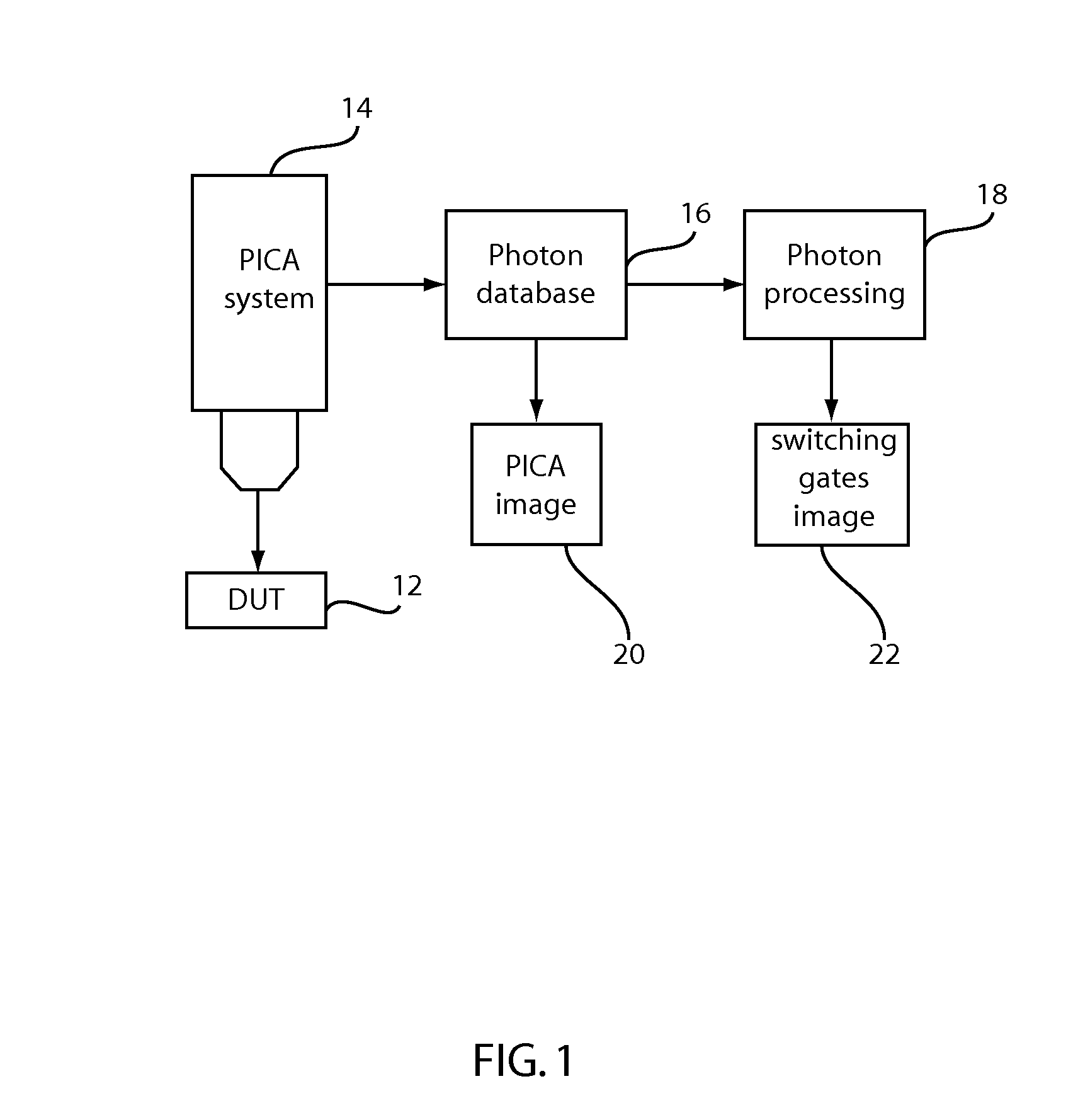
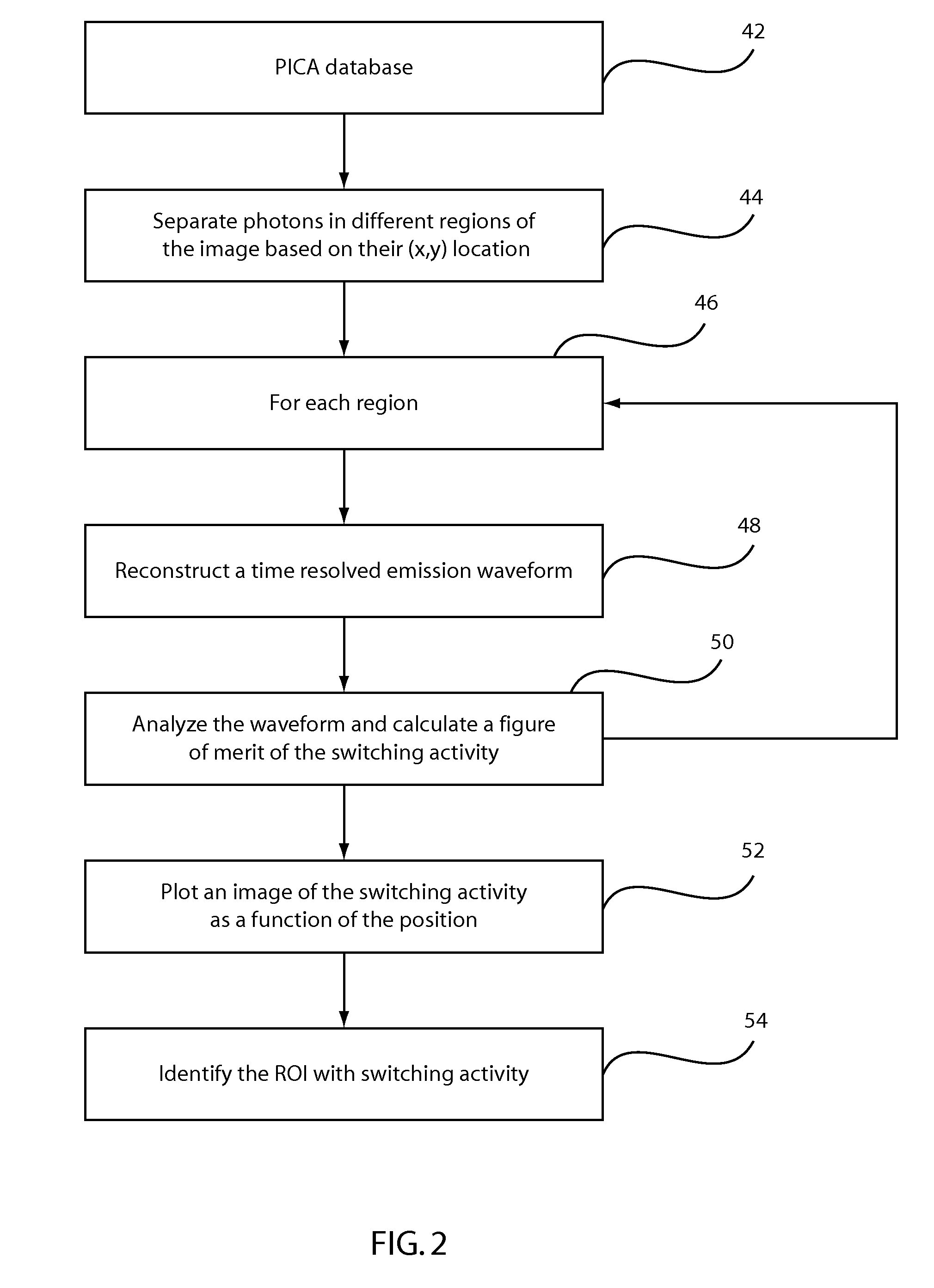
[0026]Picosecond Imaging for Circuit Analysis (PICA) is a very powerful optical methodology that permits probing time resolved emission signals collected from transistors inside a circuit. By neglecting the arrival time of the photons and constructing a spatial histogram of the measured photons one can create a “PICA image” of the emission intensity. Bright spots indicate individual transistors or sub-circuit unit composed by several transistors. By selecting a portion of the image (for example drawing a box around a region of interest) one can then create a histogram of the photon arrival time and therefore a waveform in time of the emission activity from that location.

[0027]Alternatively, 2D images of the photons at specific times can be created and then a video can be constructed by combining frames together. It should be noted that more than one bright spot is usually present in such a type of PICA image and the emission may correspond either to gates that are not switching (Lig...


PUM


Abstract

A system and method for localization and resolvability of an integrated circuit includes selecting one or more electrical stimuli to be applied to a device under test such that the electrical stimuli are chosen to provide a baseline image and a distinguishing image effect as a result of the chosen stimuli when applied to the device under test. The one or more electrical stimuli are applied to the device under test. Emissions from the device under test are measured to provide a measurement data set from the one or more electrical stimuli using one or more measurement tools for collecting the baseline image and the distinguishing image effect. The measurement data set is analyzed to localize and evaluate circuit structures by comparing the baseline image and the distinguishing image effect.

Description

BACKGROUND[0001]1. Technical Field[0002]The present invention relates to integrated circuit analysis and more particularly to a system and method for localization and resolvability of an integrated circuit using a set of stimuli to provide varying images for analyzing of the circuit.[0003]2. Description of the Related Art[0004]Analytical tools are commonly used for characterizing, testing, and debugging VLSI circuits. Some tools and techniques, such as emission tools based on off-state leakage currents and laser based stimulation tools, focus mostly on improving manufacturing process steps such as reducing leakage and variability, or improving performance and yield. Other tools and techniques, such as Time-Resolved Emission (TRE), focus mostly on probing time dependent signals from specific nodes and transistors of very large scale integration (VLSI) circuits to understand behavior and performance. In another type of application, some faulty behavior of the chip may be investigated ...

Claims


Application Information

Patent Timeline
Patent Type & Authority Applications(United States)
IPC IPC(8): G06T7/00G01R31/303
CPCG01R31/311G06T2207/30148G06T2207/10056G06T7/001G01R31/2853G06T7/11
Inventor SONG, PEILINSTELLARI, FRANCO
Owner IBM CORP
Why Eureka
Try Eureka