
Electric field shielding for in-cell touch type thin-film-transistor liquid crystal displays

a technology of in-cell touch and liquid crystal display, applied in the field of displays, can solve the problems of affecting the operation of the display, affecting the electric field of an electrostatic charge, and causing the user's finger to create large electric fields in the display,

Active Publication Date: 2011-11-24
APPLE INC
View PDF11 Cites 224 Cited by
  • Summary
  • Abstract
  • Description
  • Claims
  • Application Information

AI Technical Summary

Benefits of technology

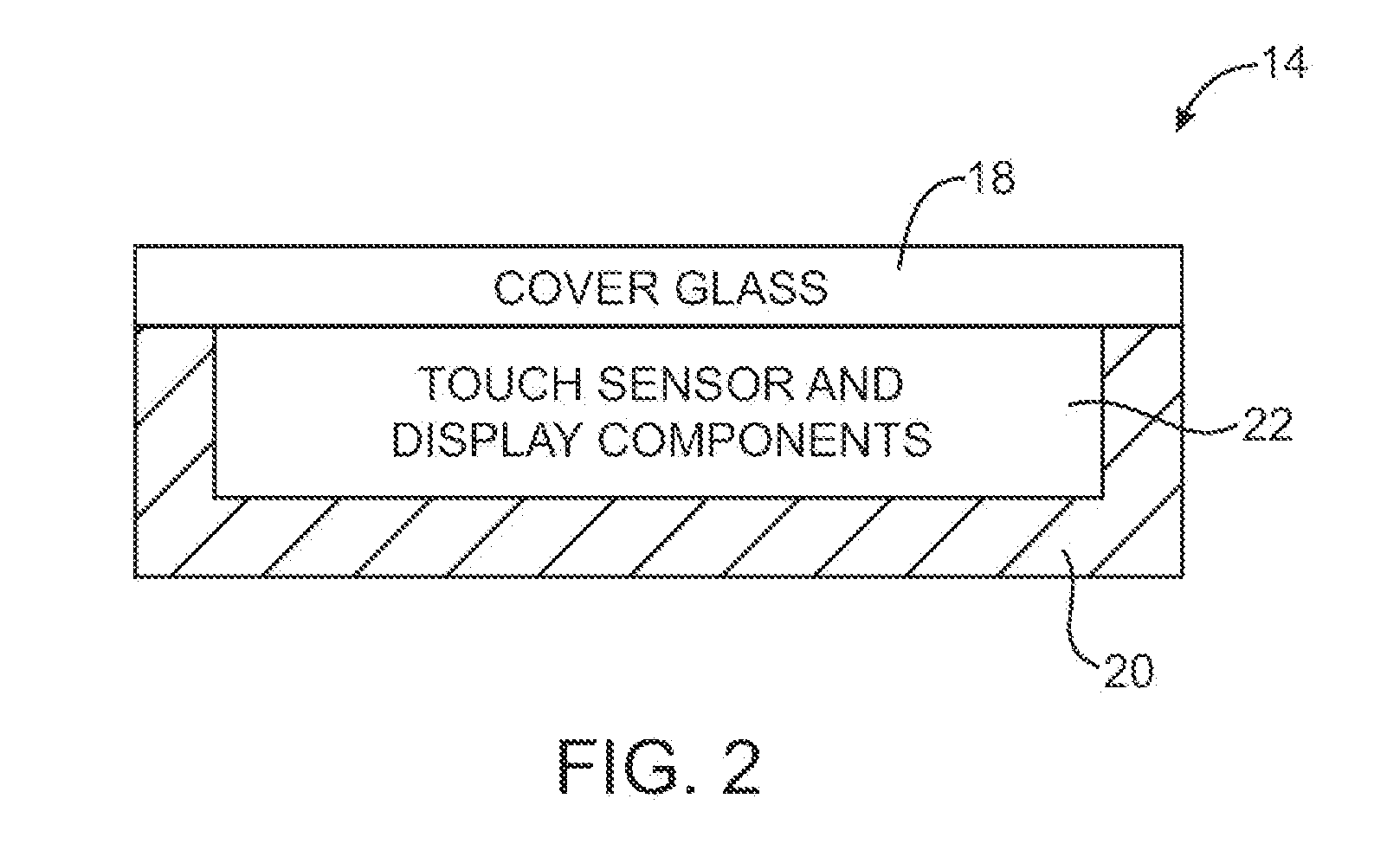
[0013]The shielding layers may be formed from conductive adhesive, metal oxides, conductive polymers, materials that include nanostructures such as carbon nanotubes, materials that include metal particles, conductive inks, or other conductive materials. The resistivity of a shielding layer may be small enough to prevent disruptions to the liquid crystal layer and large enough to avoid blocking operation of the touch sensor electrodes.
[0017]A conductive ring such as a ring of indium tin oxide may be used to help short the electric field shielding layer to a terminal such as a ground terminal on a thin-film-transistor layer.

Problems solved by technology

When an external object such as a user's finger comes into contact with a display, there is a potential for electrostatic charges on the user's finger to create large electric fields in the display.
These electric fields may disrupt the operation of the display.
For example, the electric fields from an electrostatic charge may interfere with the electric fields created by the electrodes of the thin-film-transistor layer.
This can create spots or other visual artifacts on the screen.
If care is not taken, however, the display will be susceptible to disruptions from electrostatic charge, because the touch sensor electrodes will not prevent charge-induced electric fields from reaching the liquid crystal layer.

Method used


Image

  • Electric field shielding for in-cell touch type thin-film-transistor liquid crystal displays
  • Electric field shielding for in-cell touch type thin-film-transistor liquid crystal displays
  • Electric field shielding for in-cell touch type thin-film-transistor liquid crystal displays

Examples


Embodiment Construction

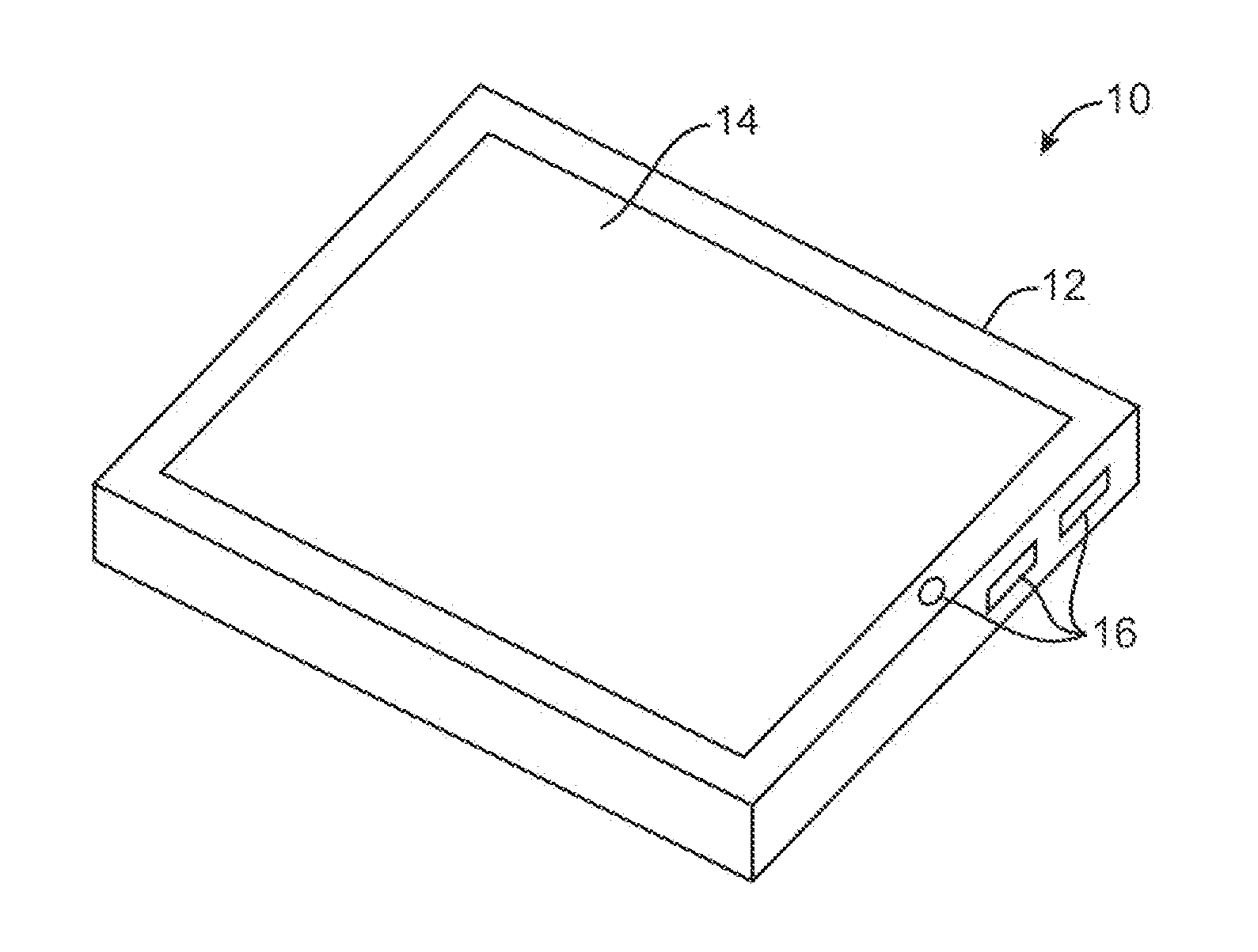
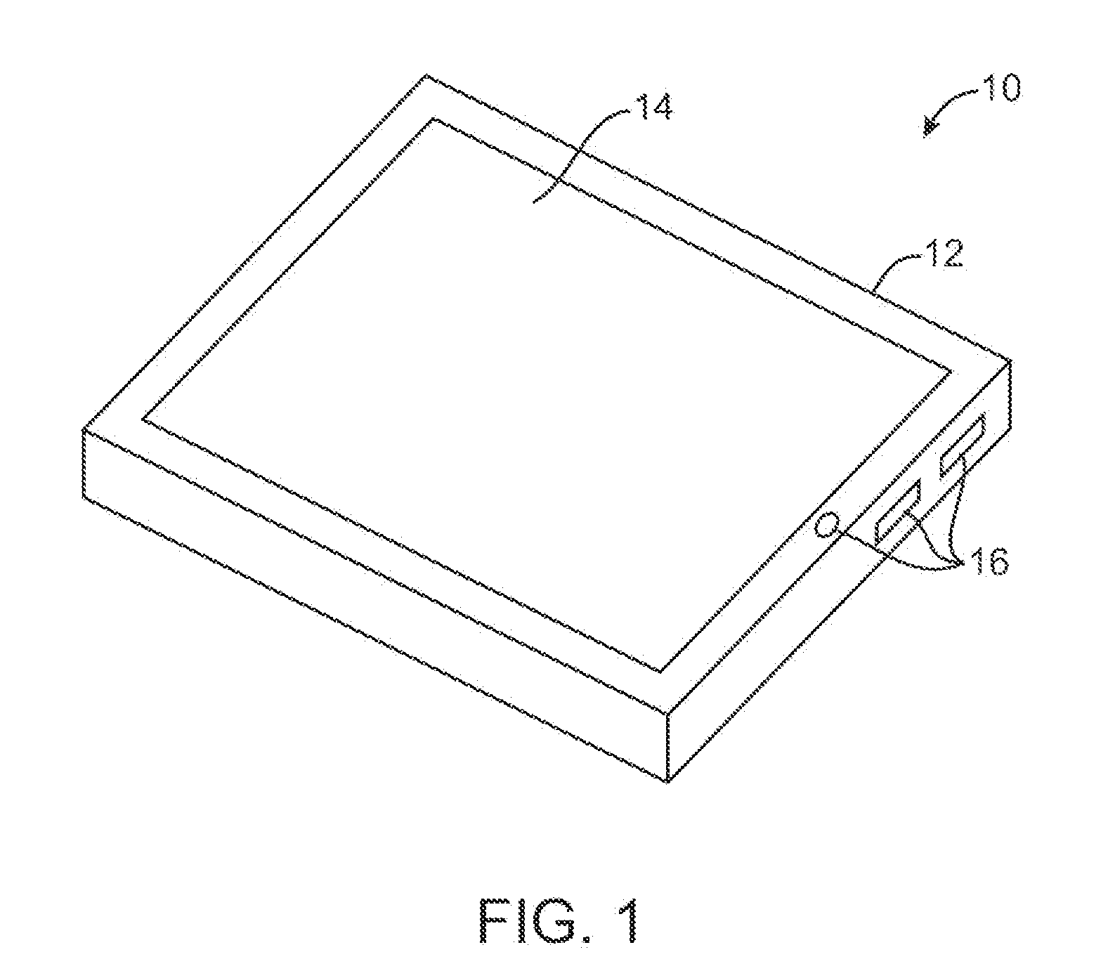
[0038]An electronic device of the type that may be provided with a display is shown in FIG. 1. As shown in FIG. 1, electronic device 10 may have a housing 12. Buttons, input-output ports, and other components 16 may be provided in housing 12. Display 14 may be mounted in housing 12 on the front surface of device 10 (as shown in FIG. 1) or may be mounted in other suitable locations within housing 12. If desired, housing 12 may have multiple sections such as first and second sections that are connected with a hinge.

[0039]Electronic device 10 may be a computer monitor for a desktop computer, a kiosk, a table-based computer, a portable computer such as a laptop or tablet computer, a media player, a cellular telephone or other handheld computing device, or may be a somewhat smaller portable device. Examples of smaller portable electronic devices include wrist-watch devices and pendant devices. These are merely examples. In general, display 14 may be incorporated into any suitable electro...


PUM


Abstract

Displays such as liquid crystal displays may be used in electronic devices. During operation of a display, electrostatic charges on the surface of the display may give rise to electric fields. One or more electric field shielding layers may be provided in the display to prevent the electric fields from disrupting operation of the liquid crystals material in the display. The shielding layers may be formed at a location in the stack of layers that make up the display that is above the liquid crystal material of the display. Touch sensors and thin film transistors may be located below the shielding layer.

Description

BACKGROUND[0001]This relates generally to displays, and, more particularly, to displays that include protective layers that prevent the operation of the display from being disrupted from electric fields.[0002]Displays are widely used in electronic devices to display images. Displays such as liquid crystal displays display images by controlling liquid crystal material associated with an array of image pixels. A typical liquid crystal display has a color filter layer and a thin film transistor layer formed between polarizer layers. The color filter layer has an array of pixels each of which includes color filter subpixels of different colors. The thin film transistor layer contains an array of thin film transistor circuits. The thin film transistor circuits can be adjusted individually for each subpixel to control the amount of light that is produced by that subpixel pixel. A light source such as a backlight may be used to produce light that travels through each of the layers of the d...

Claims


Application Information

Patent Timeline
IPC IPC(8): G06F3/041G02F1/1335G02F1/1333
CPCG02F1/13338G06F3/0412G02F2001/133334G06F2203/04107G06F3/0446G02F1/133334
Inventor PARK, YOUNG-BAEXU, MINGGE, ZHIBINGCHEN, CHENGCHANG, SHIH CHANGGETTEMY, SHAWN R.WURZEL, JOSHUA G.ZHONG, JOHN Z.
Owner APPLE INC
Learn More