Organic electroluminescent element

an electroluminescent element and organic technology, applied in the field of organic electroluminescent elements, can solve the problems of inability to achieve the practical use of blue phosphorescent materials with good power efficiency, inability to completely eliminate thermal deactivation processes without emission, and inability to achieve the effect of high emission quantum yield

Inactive Publication Date: 2011-12-01
CANON KK
View PDF2 Cites 17 Cited by
  • Summary
  • Abstract
  • Description
  • Claims
  • Application Information

AI Technical Summary

Benefits of technology

[0012]Aspects of the present invention provide an organic electroluminescent element which contai

Problems solved by technology

Until now, any blue phosphorescent material with a practical life has not been obtained.
This prevents the practical use of organic EL elements containing phosphorescent materials with good power efficiency in applications such as full-color displays and white illuminations.
However, in the organic EL element disclosed in Non-patent Document

Method used


Image

  • Organic electroluminescent element
  • Organic electroluminescent element
  • Organic electroluminescent element

Examples


example 1

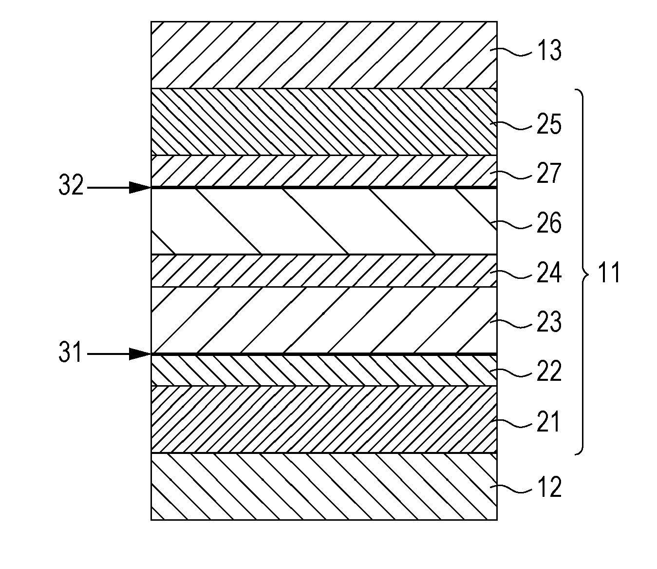
[0044]An organic EL element, having a configuration shown in FIG. 3, including an electron injection sub-layer (not shown) disposed between a cathode 13 and an electron transport sub-layer 25 was prepared by a procedure below.

[0045]A layer of an Ag alloy (Ag—Pd—Cu) used as a reflective metal was formed on a glass substrate serving as a support by a sputtering process so as to have a thickness of about 100 nm and was then patterned. An ITO layer serving as a transparent conductive film was formed on the Ag alloy layer by a sputtering process so as to have a thickness of about 20 nm and was then patterned, whereby an anode 12 serving as a reflective electrode was formed. An isolation film was formed on the anode 12 using an acrylic resin, whereby an anode-bearing substrate was prepared. The anode-bearing substrate was ultrasonically cleaned with isopropyl alcohol (IPA), was boiled in IPA, and was then dried. After the anode-bearing substrate was cleaned with UV light and ozone, an org...

example 2

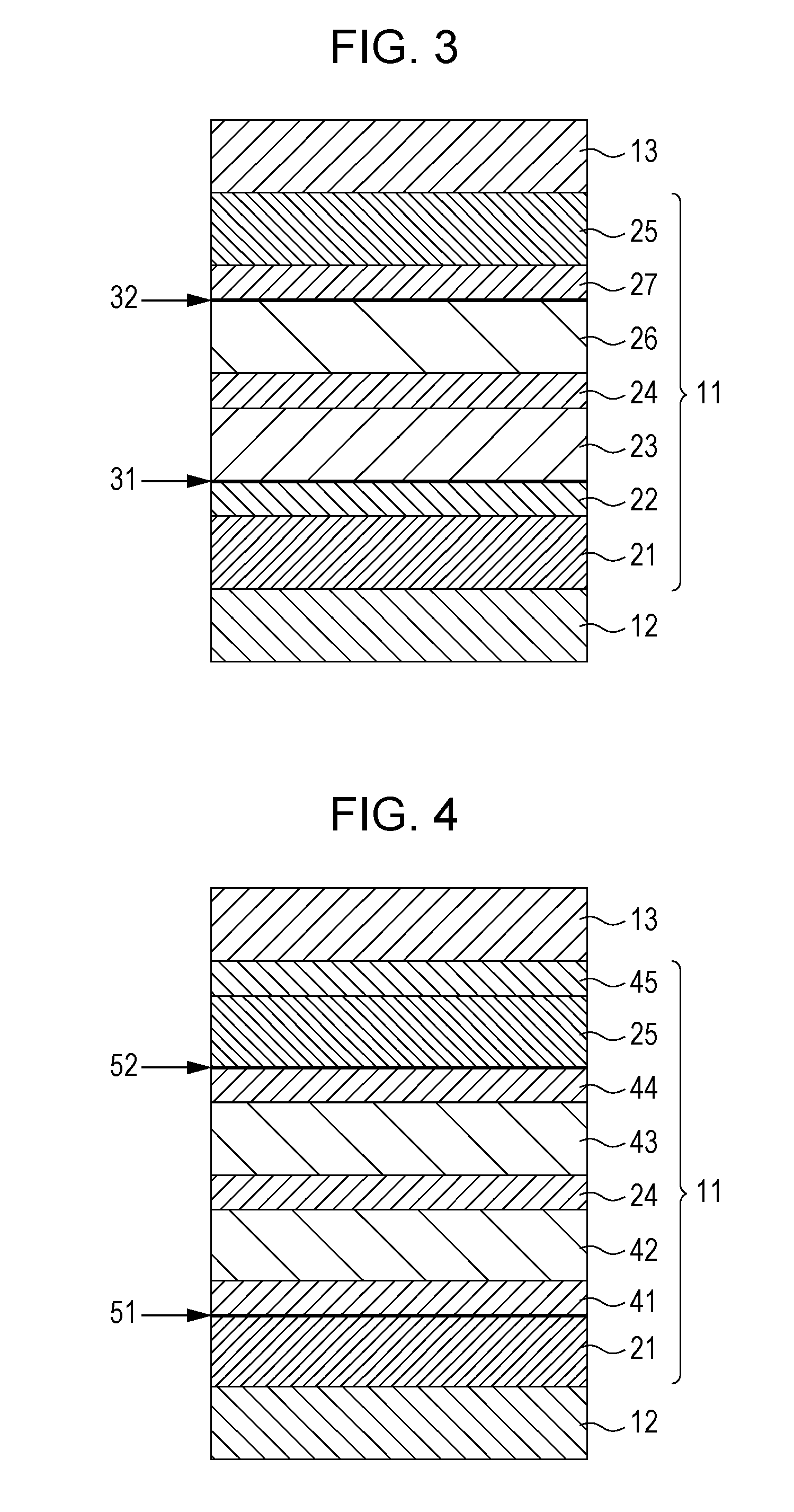
[0063]An organic EL element was prepared in substantially the same manner as that described in Example 1 except that an exciton inhibition sub-layer with a thickness of 2 nm was formed between a fluorescent light-emitting sub-layer 22 and an exciton generation sub-layer 23 using TAPC.

[0064]In the organic EL element, the LUMO of TAPC of the exciton inhibition sub-layer is 1.86 eV and the LUMO of CBP of the exciton generation sub-layer 23 is 2.54 eV. Therefore, an energy barrier for electrons is present at the interface between the exciton inhibition sub-layer and the exciton generation sub-layer 23. Electrons are accumulated on the exciton generation sub-layer 23 side of the interface and carrier recombination occurred, so that excitons are generated. Some of the accumulated electrons pass through the interface and therefore excitons are generated in a region on the exciton inhibition sub-layer side of the interface. However, this does not lead to the excitation or thermal deactivati...


PUM


Abstract

An organic compound layer includes a fluorescent light-emitting sub-layer, a phosphorescent light-emitting sub-layer, and an exciton generation sub-layer which is disposed therebetween and which generates excitons. The interface between the fluorescent light-emitting sub-layer and the exciton generation sub-layer serves as an energy barrier for carriers. Excitons are generated on the exciton generation sub-layer side of the interface therebetween.

Description

BACKGROUND OF THE INVENTION[0001]1. Field of the Invention[0002]The present invention relates to an organic electroluminescent (EL) element including a pair of electrodes and an organic compound layer which is disposed between the electrodes and which includes at least one light-emitting sub-layer.[0003]2. Description of the Related Art[0004]In recent years, many attempts have been made to develop light-emitting devices and display apparatuses including organic EL elements. In general, an organic EL element includes two electrodes and an organic compound layer which is disposed between the electrodes and which includes a light-emitting sub-layer. Examples of a luminescent material for use in the light-emitting sub-layer include fluorescent materials and phosphorescent materials.[0005]In principle, the phosphorescent materials can be expected to have higher efficiency as compared to the fluorescent materials. Because excitons generated by the recombination of carriers include singlet...

Claims


Application Information

Patent Timeline
IPC IPC(8): H01L33/02
CPCH01L51/5044H01L2251/5376H05B33/14H01L51/5028H01L51/5004H01L51/5016H01L27/32H10K50/131H10K2101/27H10K50/121H10K50/11H10K59/00H10K2101/10H10K2101/40
Inventor SHIRATORI, TSUTOMU
Owner CANON KK
Why Eureka
Try Eureka