Mitigating Signal Offsets in Optical Receivers

Active Publication Date: 2011-12-01
INFINERA CORP
View PDF4 Cites 2 Cited by
  • Summary
  • Abstract
  • Description
  • Claims
  • Application Information

AI Technical Summary

Benefits of technology

[0006]Consistent with the present disclosure, a receiver is provided which reduces signal offsets among electrical signals to provide increased capacity for optical communication systems. In one aspect, the receiver is provided with a signal processing circuit which is configured to accept two or more electrical signals. The signal processing circuit is further configured to provide an error signal indicative relative the two or more electrical signals, the error signal including a first offset signal of first magnitude. A source is provided which provides a second offset signal which is combined with the error signal to form a correction signal. The second offset signal is selected to provide the first offset signal of the error

Problems solved by technology

With the demand for increased capacity for the WDM optical communication systems, a correspondingly similar increase in complexity occurs.
When, for example, a first electrical signal having a first DC

Method used


Image

  • Mitigating Signal Offsets in Optical Receivers
  • Mitigating Signal Offsets in Optical Receivers
  • Mitigating Signal Offsets in Optical Receivers

Examples


Embodiment Construction

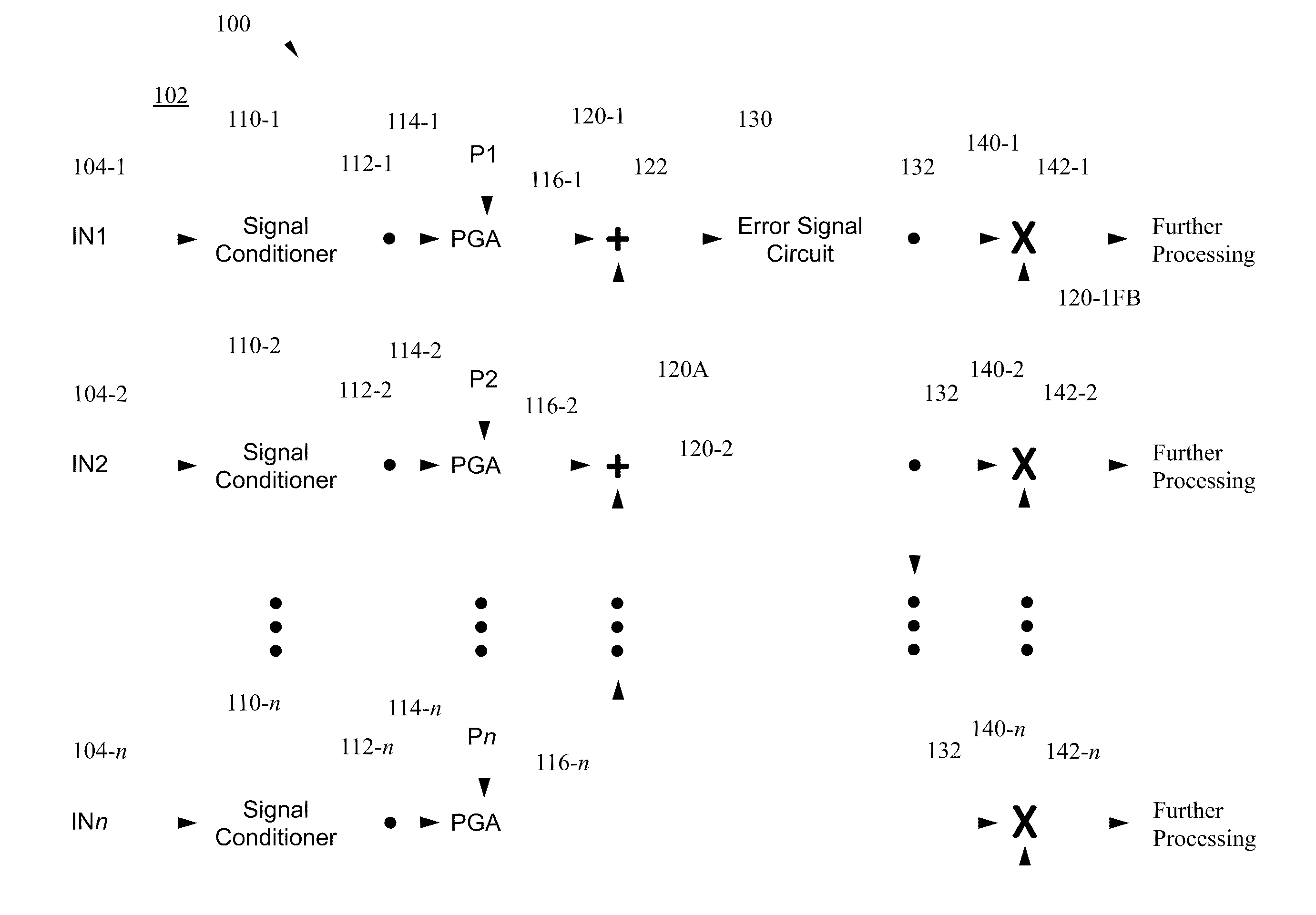
[0023]An optical receiver circuit is disclosed in which a number of electrical signals are processed to extract data encoded therein. The electrical signals may be compared during the process to selectively remove one or more waveforms from one or more corresponding electrical signals. Various data signals, each including one or more waveforms, may then be processed to extract the encoded data. The optical receiver circuit reduces, or eliminates, electrical offsets which may be present in one or more of the electrical signals to reduce errors in the processing of the encoded data signals. The optical receiver, along with other circuit components and processes, may be used to demultiplex various phase shift keying optical signals, such as quadrature phase-shift keying (QPSK), polarization quadrature phase-shift keying, or polarization multiplexed phase-shift keying signals for example.

[0024]The following description is set forth for purpose of explanation in order to provide an under...


PUM


Abstract

An optical receiver circuit is disclosed in which a number of electrical signals are processed to extract data encoded therein. The electrical signals may be compared during the process to selectively remove one or more waveforms from one or more corresponding electrical signals. Various data signals, each including one or more waveforms, may then be processed to extract the encoded data. The optical receiver circuit reduces, or eliminates, electrical offsets which may be present in one or more of the electrical signals to reduce corresponding errors in the encoded data signals.

Description

BACKGROUND OF THE INVENTION[0001]1. Field of the Invention[0002]This invention relates generally to optical telecommunication systems and, more particularly, to receivers employed in such systems.[0003]2. Description of the Related Art[0004]Wavelength-division multiplexed (WDM) optical communication systems are known in which multiple optical signals, each having a different wavelength, are combined onto a single optical fiber. With the demand for increased capacity for the WDM optical communication systems, a correspondingly similar increase in complexity occurs. For example, in order to further increase the data rates associated with WDM systems, various modulation formats have been proposed for generating the modulated laser output. One such optical signal modulation format for example, known as polarization multiplexed differential quadrature phase-shift keying (“Pol Mux DQPSK”), can provide spectral densities with higher data rates per unit of fiber bandwidth than other modulat...

Claims


Application Information

Patent Timeline
IPC IPC(8): H04B10/06
CPCH04B10/697
Inventor TSAI, HUAN-SHANGRAHN, JEFFREY T.
Owner INFINERA CORP
Why Eureka
Try Eureka