NMOS-Based Feedback Power-Clamp for On-Chip ESD Protection

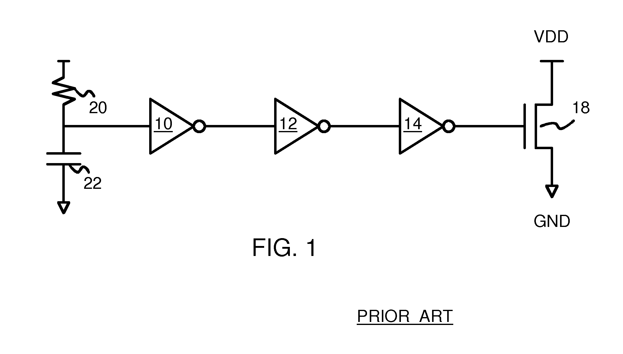
a technology of esd protection and power clamps, applied in emergency protective arrangements, electrical devices, emergency protection arrangements for limiting excess voltage/current, etc., can solve the problems of discharging esd pulses using chip internal transistors, thin oxide and insulating layers that can easily be damaged, and extremely small transistors produced by semiconductor process technology

Active Publication Date: 2011-12-08
HONG KONG APPLIED SCI & TECH RES INST
View PDF6 Cites 14 Cited by
  • Summary
  • Abstract
  • Description
  • Claims
  • Application Information

AI Technical Summary

Problems solved by technology

Semiconductor process technology produces extremely small transistors.
These tiny transistors have thin oxide and insulating layers that can easily be damaged by relatively small currents with even a moderate driving force (voltage).
When an ESD pulse was applied between Vdd and Vss, the large number of transistors connected to the power and ground supplies apparently reduced the current surge in any one device, thus dissipating the ESD pulse using the chip's internal transistors.
However, as device sizes continued to shrink, damage began occurring when ESD pulses were applied between power and ground.
The exact failure mechanism could be difficult to determine, and varied from design to design with the circuit and geometry of the integrated circuit (IC).
Damage to other thin-oxide transistors on the chip can occur before the thick-oxide transistor turns on.
Thus the protection provided by a thick-oxide transistor is less than desired.
However, a large width or base-emitter area is required to conduct enough current.
While such an active ESD-protection circuit is useful, it may be susceptible to noise, especially during power-up of the chip.
If the active ESD-protection circuit triggers during power-up, excessive current may be drawn through the clamp transistor, resulting in a drop in Vdd or even Latch-up.
Low-voltage supplies may be more susceptible since the Vdd ramp tends to be shallower.
Leakage and false triggering can be a problem with the large capacitor.

Method used


Image

  • NMOS-Based Feedback Power-Clamp for On-Chip ESD Protection
  • NMOS-Based Feedback Power-Clamp for On-Chip ESD Protection
  • NMOS-Based Feedback Power-Clamp for On-Chip ESD Protection

Examples


Embodiment Construction

[0024]The present invention relates to an improvement in ESD protection circuits. The following description is presented to enable one of ordinary skill in the art to make and use the invention as provided in the context of a particular application and its requirements. Various modifications to the preferred embodiment will be apparent to those with skill in the art, and the general principles defined herein may be applied to other embodiments. Therefore, the present invention is not intended to be limited to the particular embodiments shown and described, but is to be accorded the widest scope consistent with the principles and novel features herein disclosed.

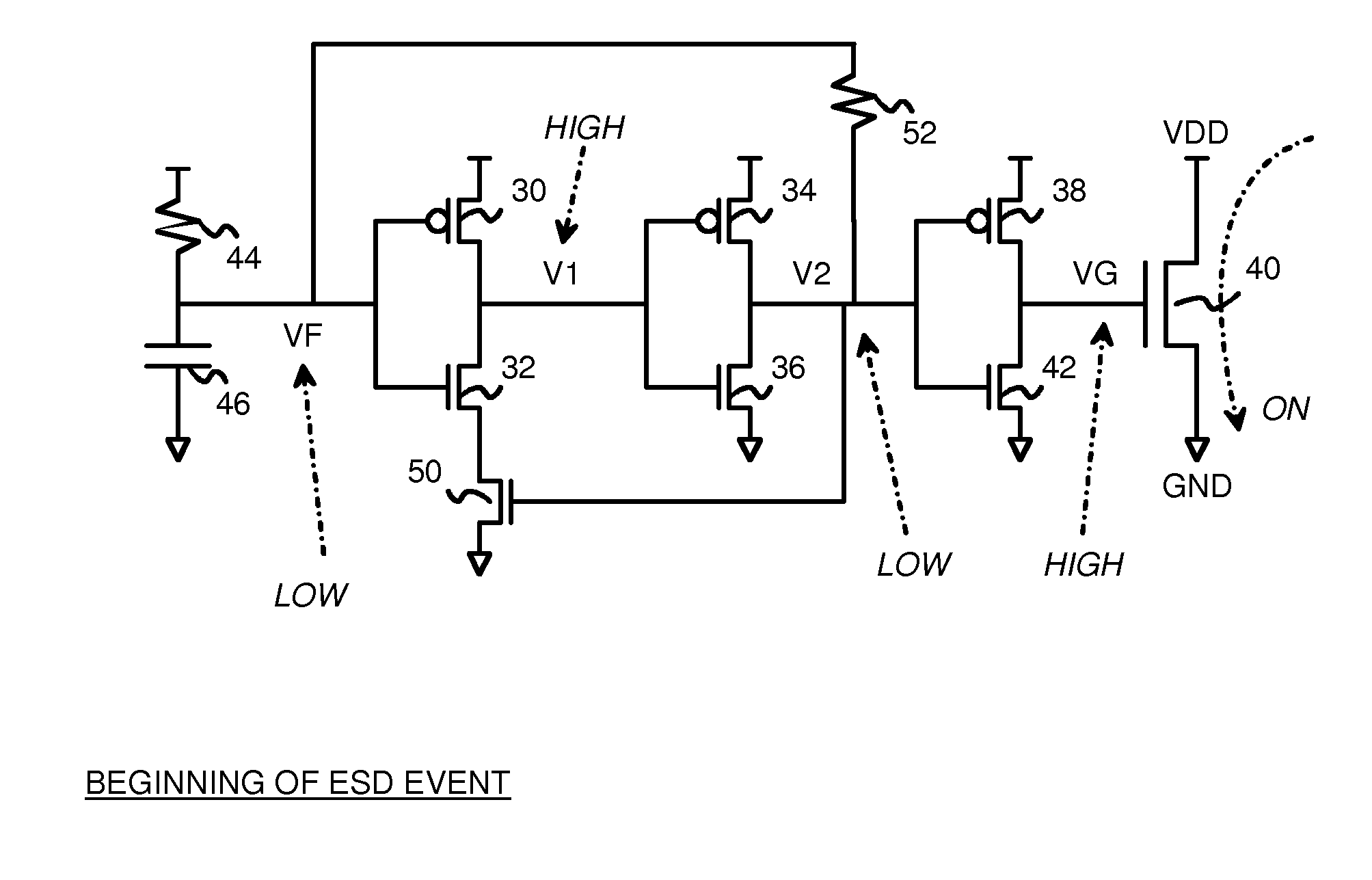
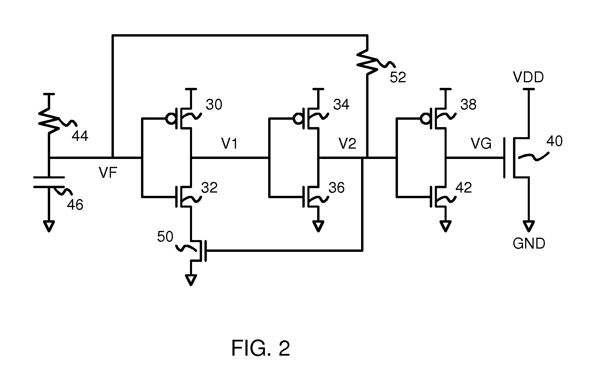
[0025]The inventors have realized that feedback can extend the time that the n-channel clamp transistor remains on, thus allowing a smaller capacitor to be used. The inventors have also realized that sub-threshold conduction can be used to further extend the turn-on time. Since sub-threshold currents are small, discharge times...


PUM


Abstract

A power-to-ground clamp transistor provides electrostatic discharge (ESD) protection. A filter capacitor and resistor generate a filter voltage that is buffered by three stages to drive the gate of the clamp transistor. The filter capacitor is about twenty times smaller than in a conventional clamp circuit. Feedback in the circuit keeps the clamp transistor turned on after the R-C time constant of the capacitor and resistor in the filer has elapsed, allowing for a smaller capacitor to turn on the clamp transistor longer. A sub-threshold-conducting transistor in the first stage conducts only a small sub-threshold current, which extends the discharge time of the first stage. The gate of the sub-threshold-conducting transistor is driven by feedback from the second stage. A feed-forward resistor has a high resistance value to slowly raise the voltage of the second stage from the filter voltage, and thus slowly raise the gate of the sub-threshold-conducting transistor.

Description

FIELD OF THE INVENTION[0001]This invention relates to electrostatic discharge (ESD) protection of semiconductor circuits, and more particularly to active feedback power-to-ground clamps.BACKGROUND OF THE INVENTION[0002]Semiconductor process technology produces extremely small transistors. These tiny transistors have thin oxide and insulating layers that can easily be damaged by relatively small currents with even a moderate driving force (voltage). Special care is required when a person handles these semiconductor devices.[0003]Static electricity that normally builds up on a person can discharge across any pair of pins of a semiconductor integrated circuit (IC or chip). IC chips are routinely tested for resistance to such electrostatic discharges (ESD) using automated testers that apply a voltage across different pairs of pins of the chip. Any pair of pins may be chosen for the ESD test. The Human Body Model (HBM) is one such test.[0004]While input and output pins were originally pr...

Claims


Application Information

Patent Timeline
Patent Type & Authority Applications(United States)
IPC IPC(8): H02H9/00
CPCH02H9/046
Inventor CAI, XAIOWUYAN, BEIPINGDU, XIAOYANGHUO, XIAOHAN, XIAOYONGYAN, BINGYONG
Owner HONG KONG APPLIED SCI & TECH RES INST
Why Eureka
Try Eureka