Interface control for improved switching in rram

a technology of interface control and rram, which is applied in the direction of digital storage, semiconductor devices, instruments, etc., can solve the problems of limiting production yields and reducing the resistance of a-si structures, and achieves the effects of facilitating filament formation, high defect density, and high defect density

Active Publication Date: 2011-12-15
INNOSTAR SEMICON SHANGHAI CO LTD
View PDF3 Cites 102 Cited by
  • Summary
  • Abstract
  • Description
  • Claims
  • Application Information

AI Technical Summary

Problems solved by technology

In the case of a-Si structures, voltage-induced diffusion of metal ions into the silicon leads to the formation of conductive filaments that reduce the resistance of the a-Si structure.
However, such devices typically have micron sized filaments which may prevent them from being scaled down to the sub-100 nanometer range.
Such devices may also require high forming voltages that can lead to device damage and can limit production yields.

Method used


Image

  • Interface control for improved switching in rram
  • Interface control for improved switching in rram
  • Interface control for improved switching in rram

Examples


Embodiment Construction

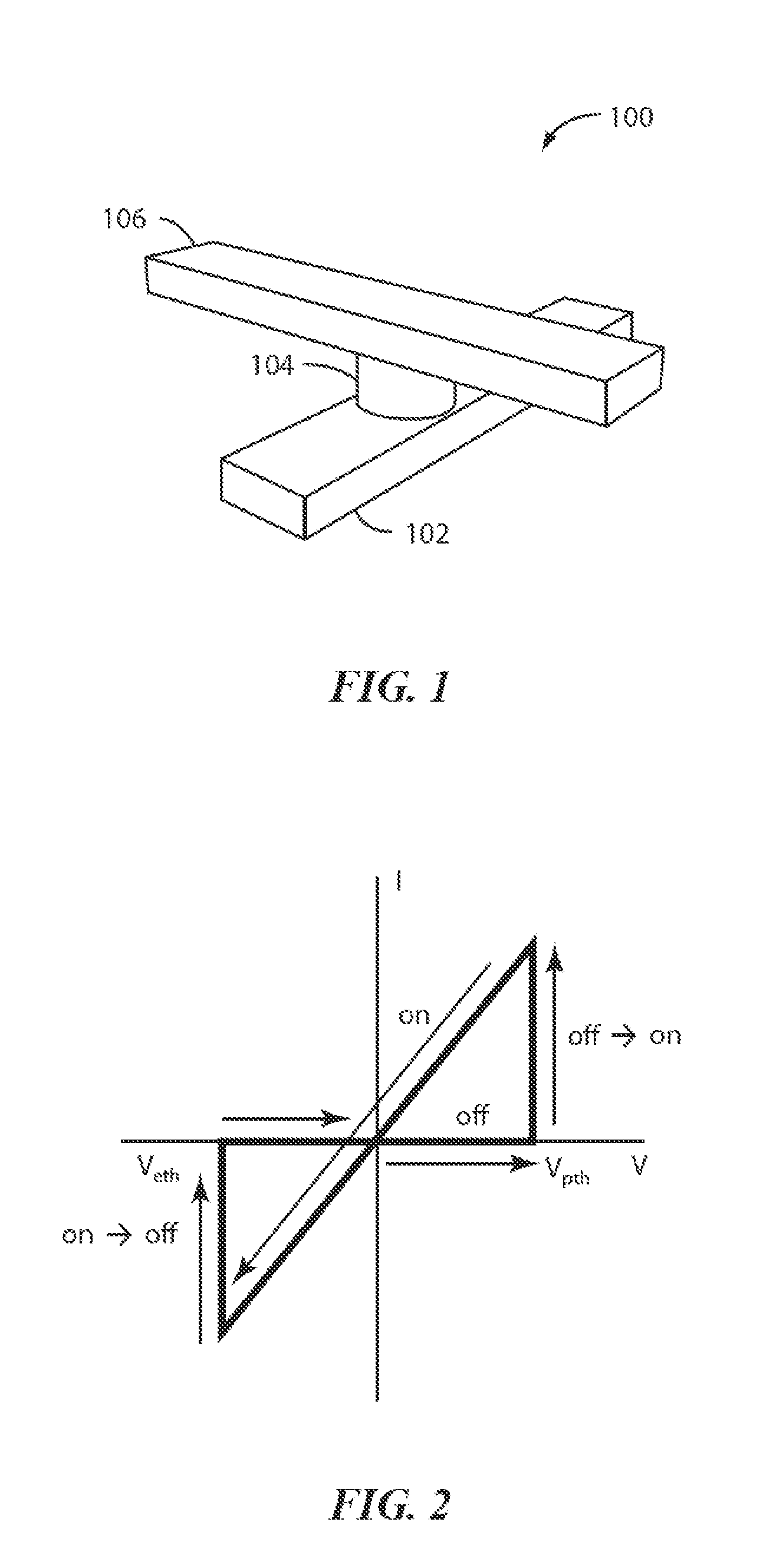
FIG. 1 illustrates a non-volatile solid state resistive device 100 including a bottom electrode 102, a switching medium 104, and a top electrode 106 according an embodiment of the present invention. Switching medium 104 exhibits a resistance that can be selectively set to various values, and reset, using appropriate control circuitry. Device 100 is a two-terminal nanoscale resistive random-access memory (RRAM) in the present embodiment. As will be appreciated by one skilled in art, device 100 may be used also as a programmable variable capacitor or other types of devices.

RRAM is a two terminal device having a switching medium provided between top and bottom electrodes. The resistance of the switching medium can be controlled by applying electrical signal to the electrodes. The electrical signal may be current-based or voltage-based. As used herein, the term “RRAM” or “resistive memory device” refers to a memory device that uses a switching medium whose resistance can be controlled b...


PUM


Abstract

A memory device has a crossbar array including a first array of first electrodes extending along a first direction. A second array of second electrodes extends along a second direction. A non-crystalline silicon structure provided between the first electrode and the second electrode at an intersection defined by the first array and the second array. The non-crystalline silicon structure has a first layer having a first defect density and a second layer having a second defect density different from the first defect density. Each intersection of the first array and the second array defines a two-terminal memory cell.

Description

CROSS-REFERENCES TO RELATED APPLICATIONSNOT APPLICABLEBACKGROUND OF THE INVENTIONThe present invention relates to solid state resistive devices used for memory storage.Resistive random-access memories (RRAMs) have generated significant interest recently as a potential candidate for ultra-high density non-volatile information storage. A typical RRAM device has an insulator layer provided between a pair of electrodes and exhibits electrical pulse induced hysteretic resistance switching effects.The resistance switching has been explained by the formation of conductive filaments inside the insulator due to Joule heating and electrochemical processes in binary oxides (e.g. NiO and TiO2) or redox processes for ionic conductors including oxides, chalcogenides and polymers. Resistance switching has also been explained by field assisted diffusion of ions in TiO2 and amorphous silicon (a-Si) films.In the case of a-Si structures, voltage-induced diffusion of metal ions into the silicon leads t...

Claims


Application Information

Patent Timeline
Patent Type & Authority Applications(United States)
IPC IPC(8): G11C11/00H01L21/02H01L45/00
CPCG11C13/0002G11C2213/33H01L27/2463H01L45/1608H01L45/1233H01L45/148H01L45/085H10B63/80H10N70/245H10N70/884H10N70/826H10N70/021
Inventor JO, SUNG HYUNNAZARIAN, HAGOPLU, WEI
Owner INNOSTAR SEMICON SHANGHAI CO LTD
Why Eureka
Try Eureka