

Semiconductor device and method for manufacturing the same
a semiconductor device and semiconductor technology, applied in the direction of semiconductor devices, semiconductor/solid-state device details, electrical apparatus, etc., can solve the problems of difficult to sufficiently stabilize the characteristics of the semiconductor device, difficult to sufficiently restrain the transmission of high-frequency signals, etc., to achieve the effect of sufficient stability
- Summary
- Abstract
- Description
- Claims
- Application Information
AI Technical Summary
Benefits of technology
Problems solved by technology
Method used
Image

Examples
first embodiment
[0035][First Embodiment]
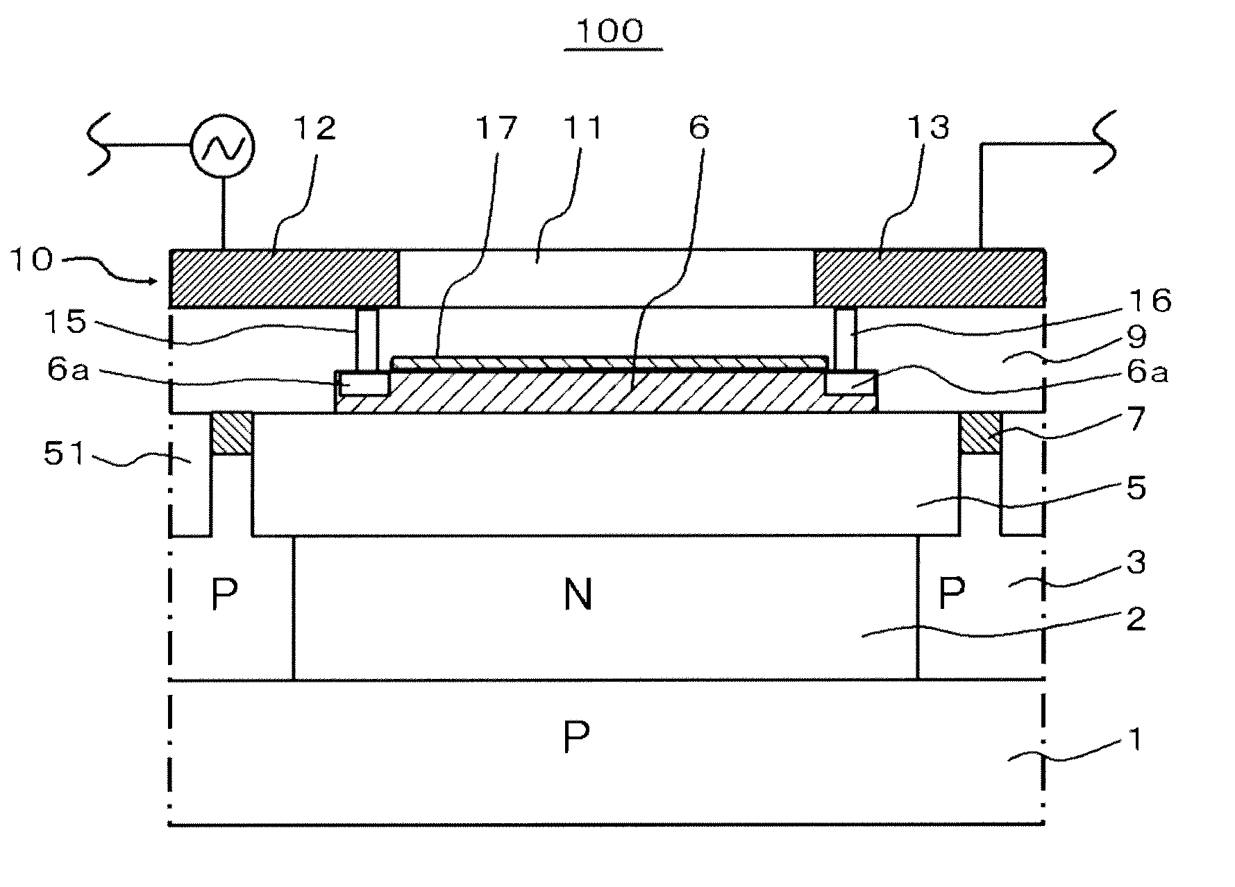
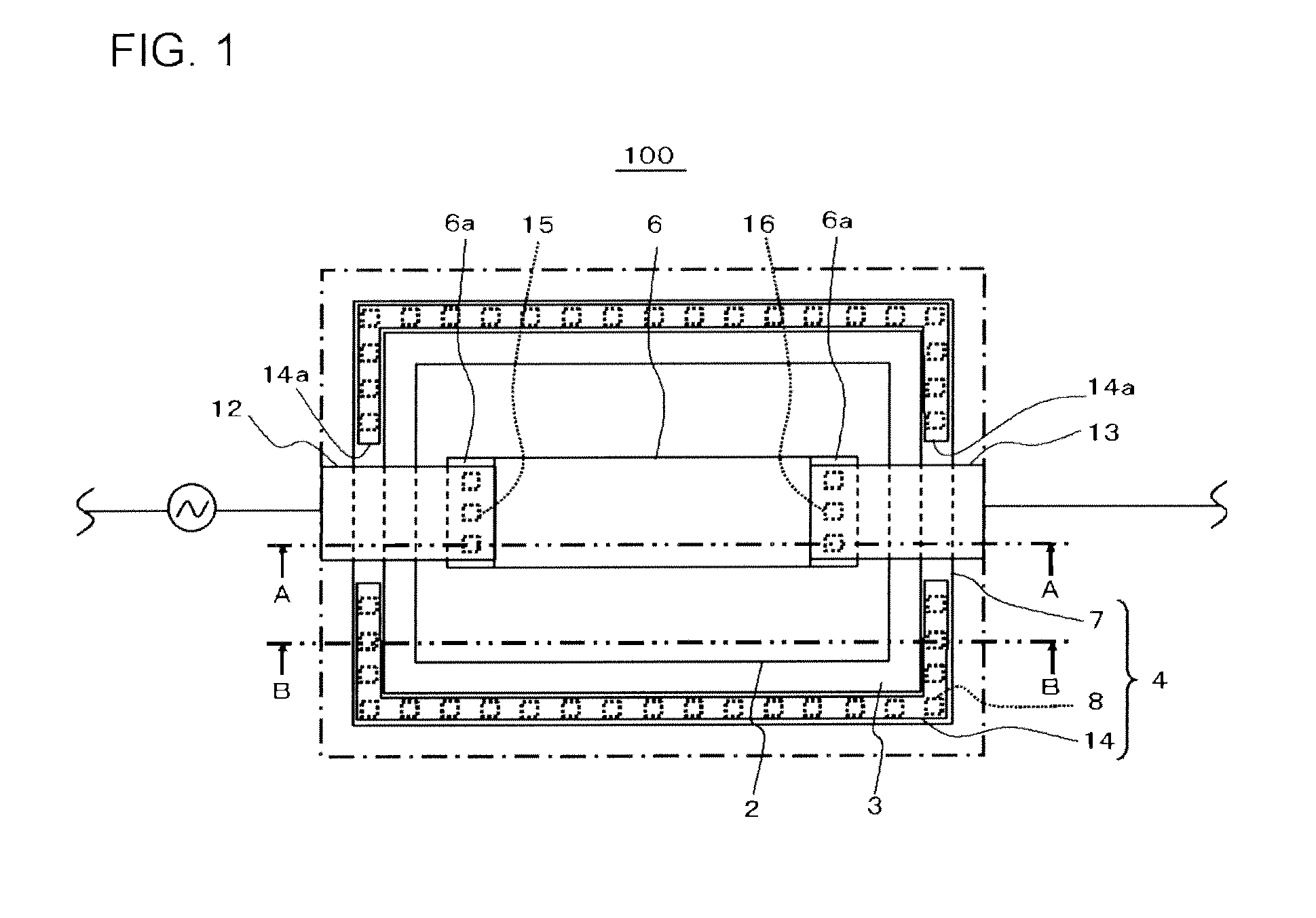
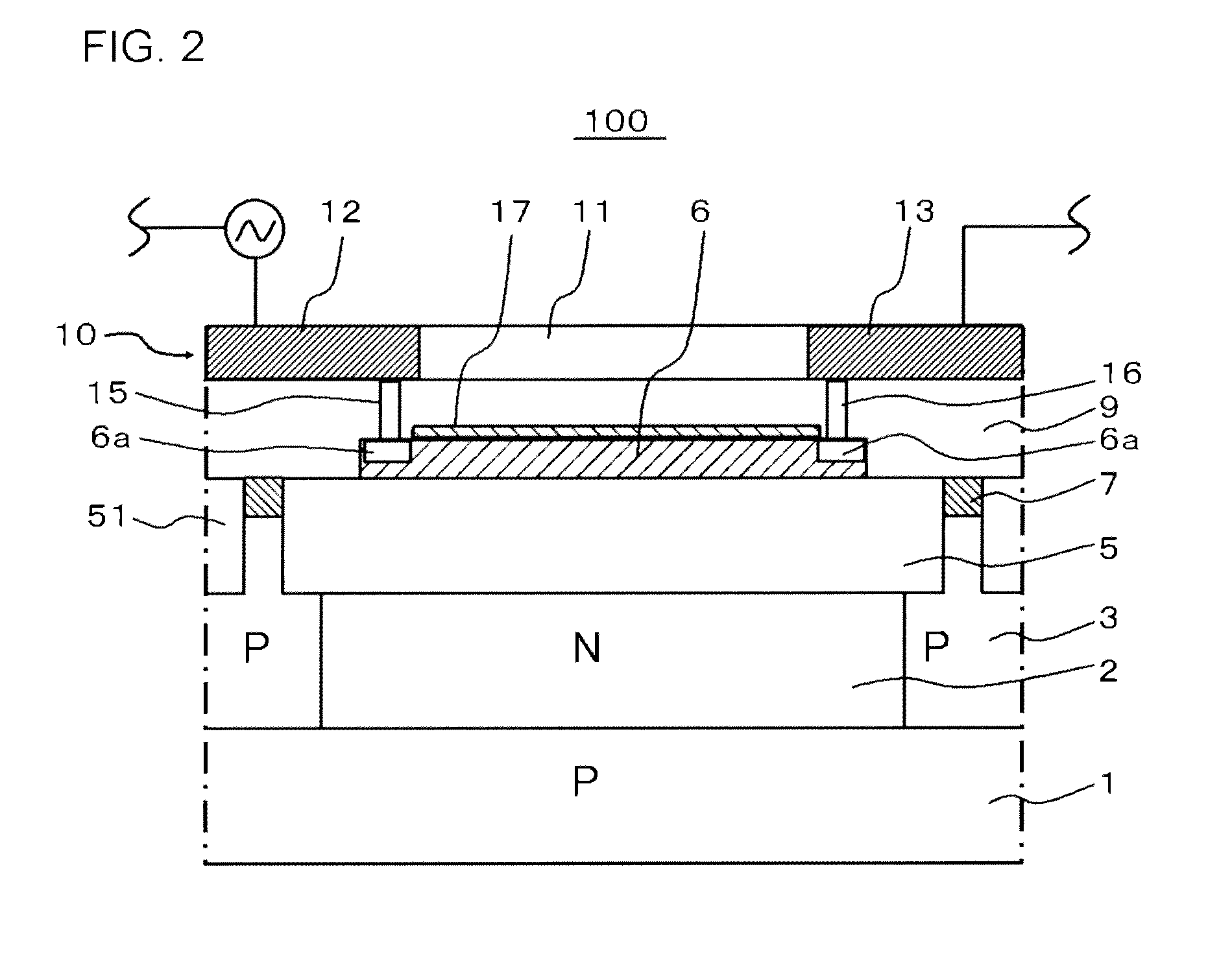
[0036]FIG. 1 is a schematic plan view of a semiconductor device 100 according to a first embodiment. FIG. 2 is a schematic cross-sectional view of the semiconductor device, taken along the line A-A of FIG. 1. FIG. 3 is a schematic cross-sectional view of the semiconductor device, taken along the line B-B of FIG. 1. In FIG. 1, an interlayer insulating film 9, an interconnect layer insulating film 11, a silicide block film 17, an insulating film 5, and an insulating film 51 are not shown.
[0037]The semiconductor device 100 according to this embodiment includes a first-conductivity-type region (an N-type well region 2, for example) and a first second-conductivity-type region (a P-type semiconductor substrate 1, for example) positioned to cover the lower surface of the first-conductivity-type region. The semiconductor device 100 further includes a second second-conductivity-type region (a P-type well region 3, for example) that is positioned to surround the side f...
second embodiment
[0107][Second Embodiment]
[0108]FIG. 7 is a plan view of a semiconductor device 200 according to a second embodiment. FIG. 8 is a schematic cross-sectional view of the semiconductor device 200, taken along the line A-A of FIG. 7. In FIG. 7, the interlayer insulating film 9, the interconnect layer insulating film 11, the silicide block film 17, the insulating film 5, and the insulating film 51 are not shown.
[0109]The semiconductor device 200 according to the second embodiment differs from the semiconductor device 100 according to the first embodiment only in the aspects described below, and the other aspects are the same as those of the semiconductor device 100.
[0110]As shown in FIGS. 7 and 8, in this embodiment, a dummy resistor 201 is provided on either side of the resistor element 6, and the resistor element 6 and the dummy resistors 201 are placed inside the guard ring 4.
[0111]Each of the dummy resistors 201 differs from the resistor element 6 only in not including the silicide re...
third embodiment
[0117][Third Embodiment]
[0118]FIG. 9 is a plan view of a semiconductor device 300 according to a third embodiment. In FIG. 9, the interlayer insulating film 9, the interconnect layer insulating film 11, the silicide block film 17, the insulating film 5, and the insulating film 51 are not shown.
[0119]The semiconductor device 300 according to the third embodiment differs from the semiconductor device 200 according to the second embodiment only in the aspects described below, and the other aspects are the same as those of the semiconductor device 200.
[0120]As shown in FIG. 9, in this embodiment, resistor elements 6 (three resistor elements 6, for example) are arranged in parallel with one another. A dummy resistor 201 is placed on either outer end of the resistor elements 6. The resistor elements 6 and the dummy resistors 201 are placed inside the guard ring 4. The respective resistor elements 6 are arranged at regular intervals. The distance between each two adjacent resistor elements...
PUM
 Abstract
Description
Claims
Application Information