Organic light emitting element and manufacturing method of the same, organic display panel, and organic display device

Active Publication Date: 2011-12-29
JOLED INC
View PDF4 Cites 9 Cited by
  • Summary
  • Abstract
  • Description
  • Claims
  • Application Information

AI Technical Summary

Benefits of technology

[0021]In the organic light emitting according to the above aspect of the present invention, a precipitate of the first metal material has been caused to form on at least part of a surface of the first electrode, and a metal oxide layer has formed in the precipitate. As described above, the first metal material included in the metal alloy composing the first electrode exhibits carrier-injection properties upon oxidation. Accordingly, the first electrode in the organic light emitting element according to the above aspect of the present invention has carrier-injection properties with respect to the functional layer, and therefore it is not necessary to form a separate carrier-injection layer on the first electrode. Omitting a carrier-injection

Problems solved by technology

However, as shown in FIG. 9, a conventional organic EL panel is formed with a large number of layers and is therefore expensive, which has led to demand for a further reduction in cos

Method used


Image

  • Organic light emitting element and manufacturing method of the same, organic display panel, and organic display device
  • Organic light emitting element and manufacturing method of the same, organic display panel, and organic display device
  • Organic light emitting element and manufacturing method of the same, organic display panel, and organic display device

Examples


embodiments

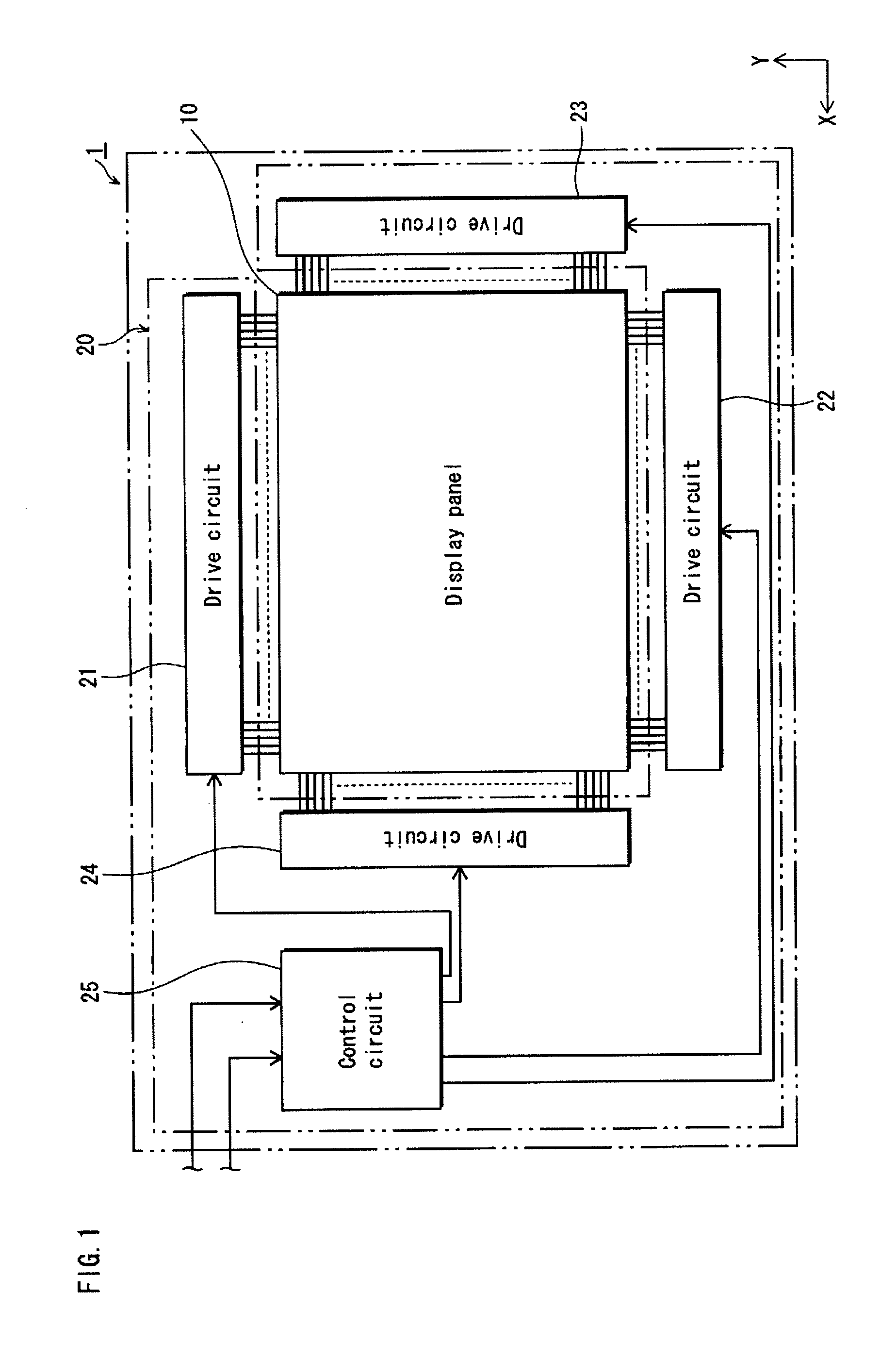
1. Overall Structure of the Display Device 1

[0061]The organic display device I according to the Embodiment is described below with reference to FIG. 1.

[0062]As shown in FIG. 1, the organic display device 1 is composed of an organic display panel unit 10 and a drive control unit 20 connected to the organic display panel unit 10. The organic display panel unit 10 is an organic EL panel that uses the phenomenon of electroluminescence occurring in organic light emitting material and is composed of an array of a plurality of organic light emitting elements.

[0063]The drive control unit 20 is composed of four drive circuits 21-24 and a control circuit 25.

[0064]Note that in an actual display device 1, the placement and relation of connection of the drive control unit 20 with respect to the display panel unit 10 is not limited in this way.

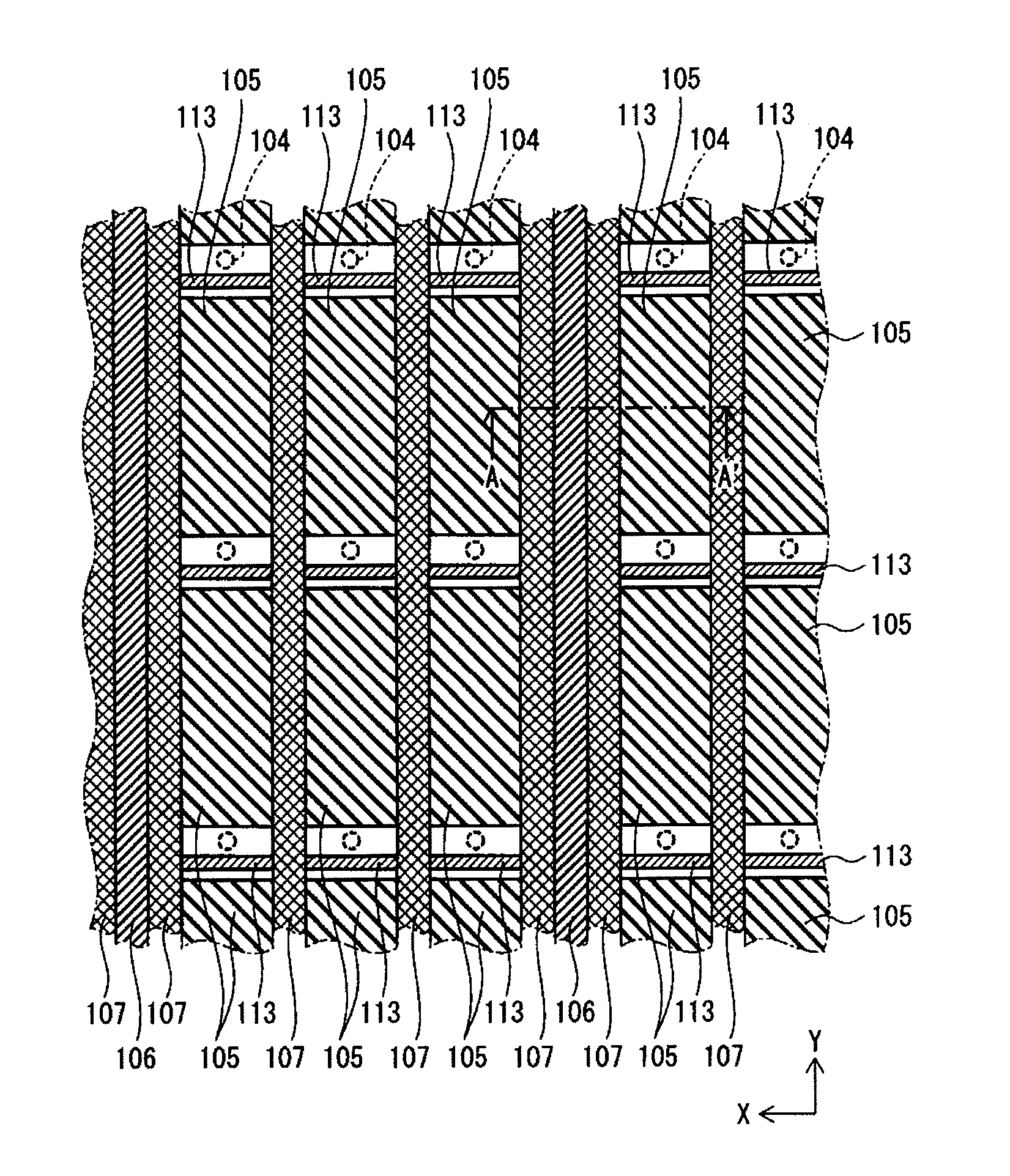
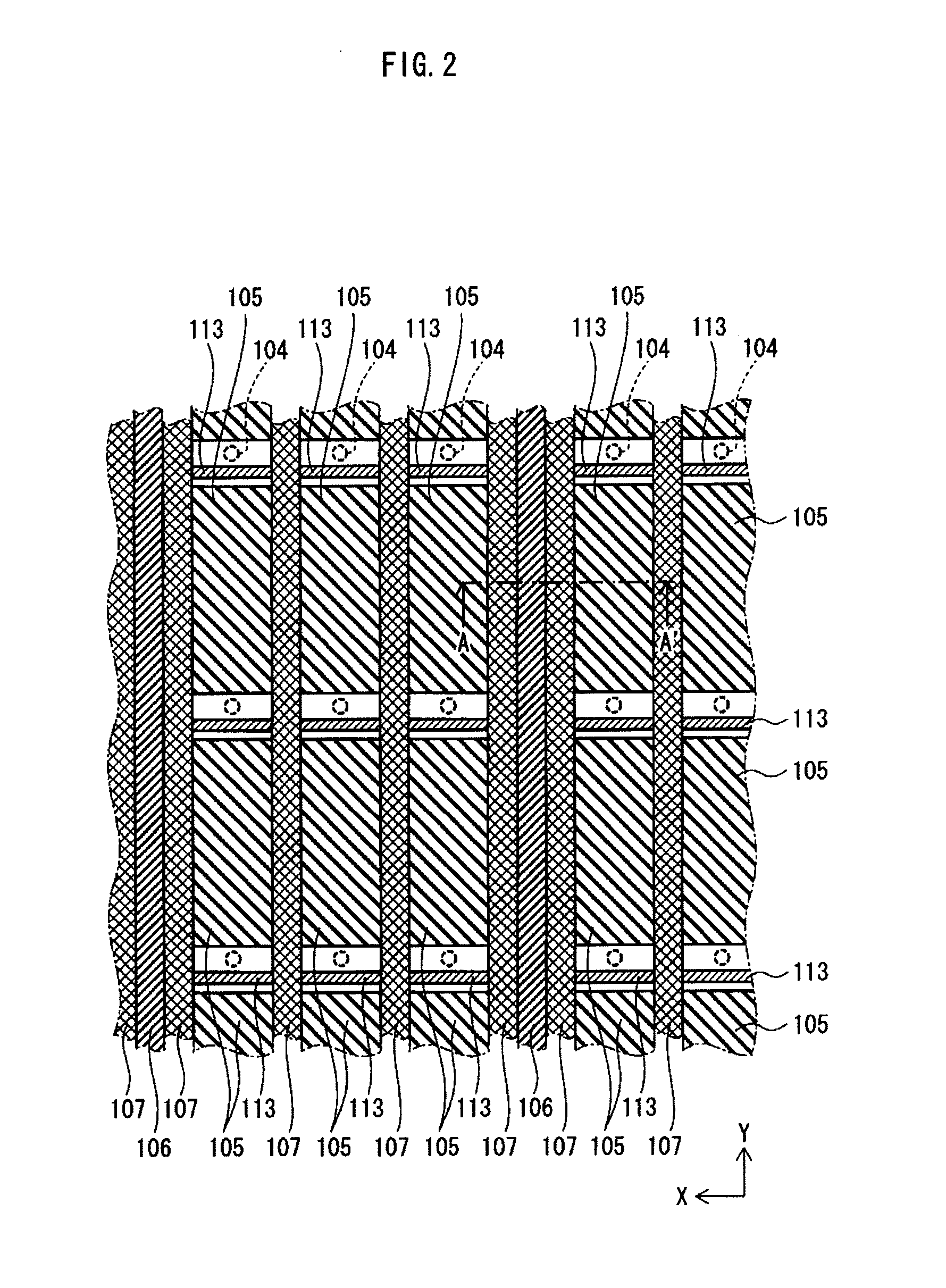
2. Structure of Organic Display Panel 10

[0065]The structure of the organic display panel 10 is described with reference to FIGS. 2 and 3. FIG. 2 is a schem...


PUM


Abstract

An organic light emitting element and method for manufacturing an organic light emitting element. A first electrode is formed from a metal alloy that includes a first metal material that exhibits a carrier-injection property upon oxidation, and a second metal material that is light-reflective and electrically conductive, a precipitate of the first metal material forming on at least part of a surface of the first electrode, and a metal oxide layer being formed in the precipitate. A functional layer contacts the surface of the first electrode and includes at least a light-emitting layer configured to accept a carrier injected by the first electrode. A second electrode is disposed opposite the first electrode with the functional layer therebetween and has a polarity different from a polarity of the first electrode.

Description

CROSS REFERENCE TO RELATED APPLICATION[0001]This is a continuation application of PCT Application No. PCT / JP2010 / 004264 filed Jun. 28, 2010, designating the United States of America, the disclosure of which, including the specification, drawings and claims, is incorporated herein by reference in its entirety.BACKGROUND OF THE INVENTION[0002]1. Field of the Invention[0003]The present invention relates to organic light emitting elements and a manufacturing method of the same, organic display panels, and organic display devices.[0004]2. Description of Related Art[0005]In recent years, progress has been made in the research and development of organic electroluminescent elements (hereinafter, “organic EL elements”), which are light-emitting elements that rely on the phenomenon of electroluminescence of organic material. The structure of an organic EL panel that uses conventional organic EL elements is described with reference to FIG. 9.[0006]As shown in FIG. 9, a thin-film transistor lay...

Claims


Application Information

Patent Timeline
IPC IPC(8): H01J1/62H01J9/00
CPCH01L27/3244H01L51/0021H05B33/10H01L51/5228H01L2251/55H01L51/5218H10K59/12H10K71/60H10K50/818H10K50/824H10K2101/00H10K50/14
Inventor NENDAI, KENICHI
Owner JOLED INC
Why Eureka
Try Eureka