Thin film balun

a balun and thin film technology, applied in the direction of electrical devices, coupling devices, impedence networks, etc., can solve the problems of insufficient balun characteristics and insufficient desired balanced characteristics, and achieve excellent balanced characteristics, maintain miniaturization, and change the impedance of the circuit

Active Publication Date: 2011-12-29
TDK CORPARATION
View PDF6 Cites 3 Cited by
  • Summary
  • Abstract
  • Description
  • Claims
  • Application Information

AI Technical Summary

Benefits of technology

[0021]According to the present invention, by configuring such that the ground terminal has an extension that extends from the ground terminal to an area at the unbalanced terminal side, a thin film balun with excellent balanced characteristics while maintaining miniaturization may be obtained. In addition, by providing an L component between the third line portion and the fourth line portion described above in the thin film balun, the impedance of the circuit is changed and the impedance matching characteristic is improved, and as a result, the electrical characteristics of the thin film balun can be remarkably improved.

Problems solved by technology

However, in the configuration of a chip-type balun disclosed in the above patent document 1, a desired balanced characteristic cannot be sufficiently obtained in a signal frequency that is to be converted while maintaining miniaturization of the balun, and there is a problem in that the characteristic of the balun is insufficient as a balun for high frequency used in mobile phones, etc.

Method used


Image

  • Thin film balun
  • Thin film balun
  • Thin film balun

Examples


example 1

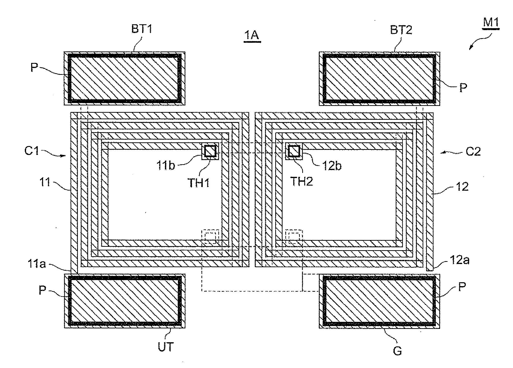
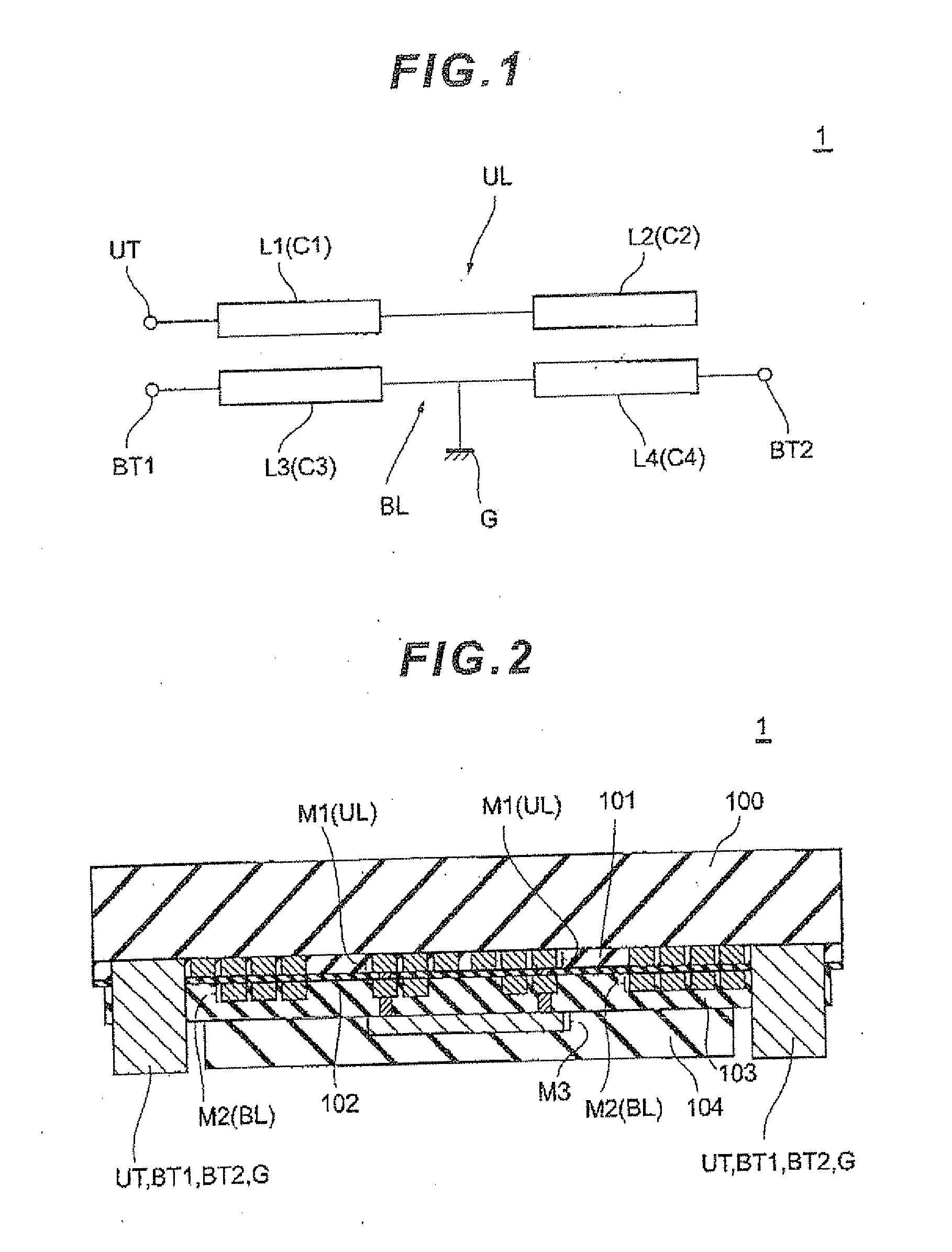
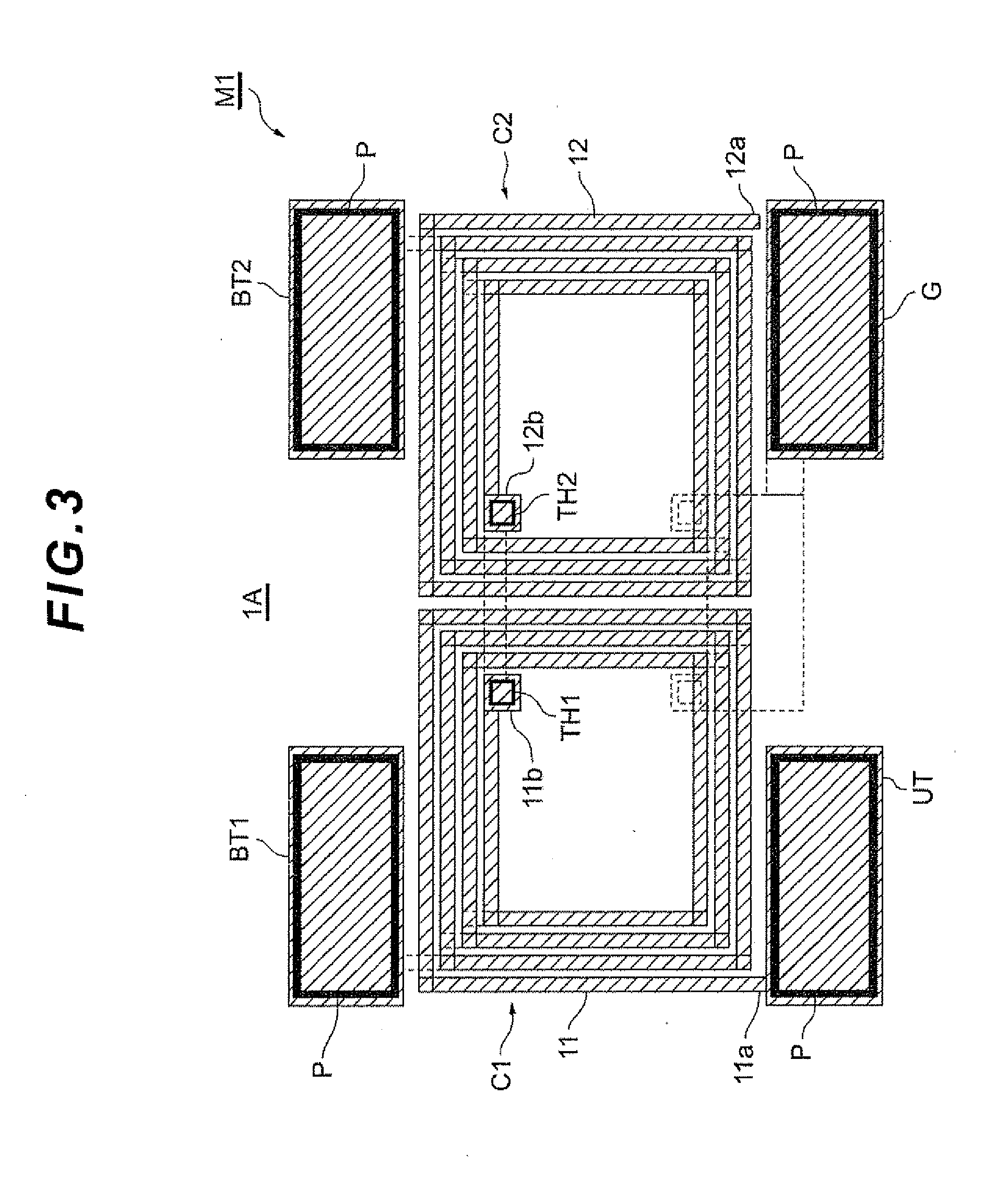
[0070]A pattern of each of the wiring layers M1, M2 and M3 in an example of the thin film balun of the present embodiment is described in detail below. Coil portions C1 to C4 are used as the line portions L1 to L4 in the following example.

[0071]FIGS. 3 to 5 are horizontal sectional views schematically showing each wiring layer in the thin film balun 1A of Example 1 of the present invention. As shown in FIGS. 3 to 5, the unbalanced terminal UT, the balanced terminals BT1 and BT2 and the ground terminal G are formed in all of the wiring layers M1 to M3, and each of the terminals UT, BT1, BT2 and G is electrically connected between different layers via a through hole P. Through holes TH1 to TH4 shown in FIGS. 3 to 5 are plated with a metal conductor for electrical conduction of upper and lower layers. A configuration of each of the wiring layers M1 to M3 is further described below.

[0072]As shown in FIG. 3, a coil portion C1 (first line portion) and the coil portion C2 (second line port...

example 2

[0081]FIG. 6 is a horizontal sectional view schematically showing the wiring layer M3 in the thin film balun 1B of Example 2 of the present invention. The configuration other than that of the wiring layer M3 is the same as Example 1. As shown in FIG. 6, in contrast to the GND electrode 40A of Example 1, the GND electrode 40B of the thin film balun 1B is formed at a position that excludes the area facing the coil portions C3 and C4 that constitute the balanced transmission line BL. That is, the GND electrode40B is formed at an area which does not overlap with the coil portions C3 and C4. The GND electrode 40B extends from the ground terminal G to an area near the unbalanced terminal UT and is electrically connected to each of the wirings (lead conductors) 32 and 33 of the coil portions C3 and C4 via the through holes TH3 and TH4 of the wiring layer M3.

example 3

[0082]FIG. 7 is a horizontal sectional view schematically showing the wiring layer M3 in the thin film balun 1C of Example 3 of the present invention. The configuration other than that of the wiring layer M3 is same as Example 1. As shown in FIG. 7, in contrast to the GND electrode 40A of the thin film balun 1A, the GND electrode 40C of the thin film balun 1C is formed at a position of the area facing each part of the coil portions C3 and C4 that constitute the wiring layer M2. The area of the GND electrode 40C is greater than the area of the GND electrode 40A.


PUM


Abstract

A thin film balun of the present invention comprises: an unbalanced transmission line UL including a first line portion L1 and a second line portion L2; a balanced transmission line BL including a third line portion L3 and a fourth line portion L4 that are positioned facing the first line portion L1 and the second line portion L2 and electromagnetically coupled to the first line portion L1 and the second line portion L2, respectively; an unbalanced terminal UT connected to an end of the first line portion L1; a first balanced terminal BT1 connected to the third line portion L3; a second balanced terminal BT2 connected to the fourth line portion L4; and a ground terminal G connected to the third line portion L3 and the fourth line portion L4, wherein the ground terminal G has an extension that extends from the ground terminal G to an area at the unbalanced terminal UT side.

Description

CROSS-REFERENCES TO RELATED APPLICATIONS[0001]The present application claims priority to prior filed Japanese Patent applications No. 2010-145097, filed on Jun. 25, 2010 and No. 2010-170435, filed on Jul. 29, 2010, the entire contents of which are hereby incorporated by reference.FIELD OF THE INVENTION[0002]The present invention relates to a balun (balun transformer) that performs conversion between unbalanced and balanced signals, in particular to a thin film balun that is formed by a thin film process advantageous for smaller and thinner models.BACKGROUND OF THE INVENTION[0003]A wireless communication device comprises various high frequency elements such as an antenna, a filter, an RF switch, a power amplifier, an RF-IC and a balun. Of these elements, a resonant element such as an antenna or a filter handles (transmits) an unbalanced signal which is based on a ground potential, whereas an RF-IC which generates or processes a high frequency signal handles (transmits) a balanced sig...

Claims


Application Information

Patent Timeline
Patent Type & Authority Applications(United States)
IPC IPC(8): H01P5/10
CPCH01P5/10
Inventor ENDO, MAKOTO
Owner TDK CORPARATION
Why Eureka
Try Eureka