Electroplating methods and chemistries for cigs precursor stacks with conductive selenide bottom layer

a technology of cigs precursor stack and selenide bottom layer, which is applied in the direction of photovoltaic energy generation, semiconductor devices, electrical equipment, etc., can solve the problems of high cost of capital equipment, relatively slow production rate, and high cost of silicon-based solar cells. achieve the effect of rapid thermal annealing

Inactive Publication Date: 2012-01-05
SOLOPOWER
View PDF4 Cites 9 Cited by
  • Summary
  • Abstract
  • Description
  • Claims
  • Application Information

AI Technical Summary

Problems solved by technology

However, the cost of electricity generated using silicon-based solar cells is higher than the cost of electricity generated by the more traditional methods.
Such techniques may yield good quality absorber layers and efficient solar cells, however, they suffer from the high cost of capital equipment, and relatively slow rate of production.
Gallium addition in the quaternary layers was very challenging in the latter attempts.

Method used


Image

  • Electroplating methods and chemistries for cigs precursor stacks with conductive selenide bottom layer
  • Electroplating methods and chemistries for cigs precursor stacks with conductive selenide bottom layer

Examples


Embodiment Construction

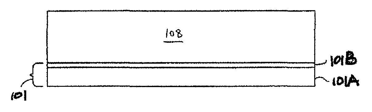
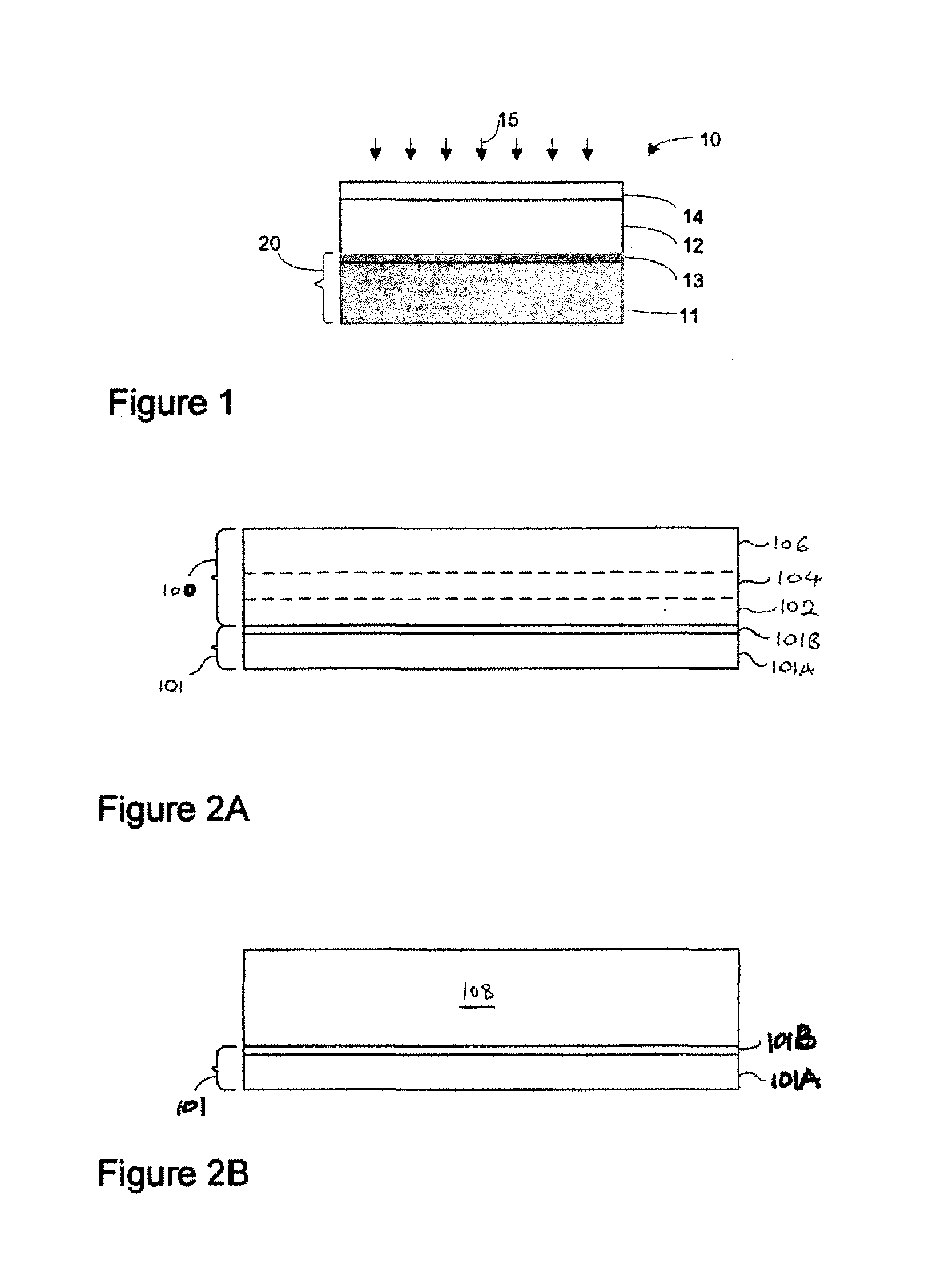
[0021]The present invention provides various methods to form Cu(In, Ga) (Se, S)2 absorber layers (CIGS) from electrodeposited precursors of the present invention. A precursor of the present invention may be formed as a stack having three layers. A first layer, which is copper poor, may be deposited over a base and a second layer, which is copper rich, deposited onto the first layer. A third layer including selenium is deposited onto the second layer before reacting the precursor to form the CIGS absorber layer. The first layer may include a Group IB-Group IIIA alloy or mixture of stacked films where the Group IB material is preferably Cu and the Group IIIA material is at least one of In and Ga. Such films may include (Cu—In), (Cu—Ga) and (Cu—In—Ga) alloy films or mixture such films. Alternatively, the first layer may include a mixture of stacked single element films, i.e., Cu, In, Ga films, or a mixture of such single element films and (Cu—In), (Cu—Ga) and (Cu—In—Ga) alloy films. Th...


PUM

PropertyMeasurementUnit
temperatureaaaaaaaaaa
molar ratioaaaaaaaaaa

Abstract

The present invention provides a method and precursor structure to form a solar cell absorber layer. The method includes forming a CIGS solar cell absorber on a base by depositing a first layer on the base, where in the first layer includes non-crystalline copper-selenide that is electrically nonconductive, and then heat treating the first layer at a first temperature range to transform the non-crystalline copper-selenide into a crystalline copper-selenide that is electrically conductive, thereby ensuring that the first layer becomes a first conductive layer. Thereafter, other steps follow to complete formation of the CIGS solar cell absorber.

Description

CROSS REFERENCES TO RELATED APPLICATIONS[0001]This application is a Continuation-in-Part of U.S. patent application Ser. No. 12 / 642,702, filed on Dec. 18, 2009 entitled “ELECTROPLATING METHODS AND CHEMISTRIES FOR DEPOSITION OF COPPER-INDIUM-GALLIUM CONTAINING THIN FILMS” (SP-101), and this application is a Continuation in Part of U.S. patent application Ser. No. 12 / 642,709 filed on Dec. 18, 2009 entitled “ENHANCED PLATING CHEMISTRIES AND METHODS FOR PREPARATION OF GROUP IBIIIAVIA THIN FILM SOLAR ABSORBERS” (SP-098), and this application is a Continuation in Part of U.S. patent application Ser. No. 12 / 642,691 filed on Dec. 18, 2009 entitled “SELENIUM CONTAINING ELECTRO DEPOSITION SOLUTIONS AND METHODS”, (SP-103), and this application is a Continuation in Part of U.S. patent application Ser. No. 11 / 952,905 filed on Dec. 7, 2007 entitled “ELECTRODEPOSITION TECHNIQUE AND APPARATUS TO FORM SELENIUM CONTAINING LAYERS” (SP-021), all of which are expressly incorporated herein by reference)B...

Claims


Application Information

Patent Timeline
Patent Type & Authority Applications(United States)
IPC IPC(8): H01L31/18
CPCC25D3/38C25D3/54C25D3/58C25D5/10C25D5/50Y02E10/541H01L21/02568H01L21/02614H01L21/02628H01L31/0322H01L21/02491C25D5/619C25D5/611
Inventor AKSU, SERDARPINARBASI, MUSTAFA
Owner SOLOPOWER
Why Eureka
Try Eureka