Light Emissive Device

a light emissive device and light emissive technology, applied in the direction of discharge tube luminescnet screens, electric discharge lamps, electrical equipment, etc., can solve the problems of high damage to cathode and light emitting layer, adverse effects on cathode transparency, and high damage to cathode and other problems, to achieve the effect of improving the stability of the electrode, low reactivity, and high work function materials

Active Publication Date: 2012-01-12
CAMBRIDGE DISPLAY TECH LTD
View PDF4 Cites 6 Cited by
  • Summary
  • Abstract
  • Description
  • Claims
  • Application Information

AI Technical Summary

Benefits of technology

[0011]The invention provides an organic light emissive device with improved properties, including a cathode with improved electron injection into the organic light emissive region, and also provides a cathode capable of injecting electrons into a variety of different types of organic light emissive materials, i.e., a “common electrode,” so that electron-injection into red, green and blue light organic emissive materials can be effected with a single cathode.

Problems solved by technology

A problem arises with the fabrication of the cathode of this arrangement.
However, sputtering is a highly damaging process and if the ITO were sputtered directly onto an unprotected barium cathode, the cathode and light emitting layer would be damaged.
However, in order to achieve the buffering protection required, a relatively high thickness of metal would need to be used and this may have adverse effects on the transparency of the cathode.
These buffer materials, however, suffer from a disadvantage that they are poor conductors.

Method used


Image

  • Light Emissive Device
  • Light Emissive Device
  • Light Emissive Device

Examples


example 1

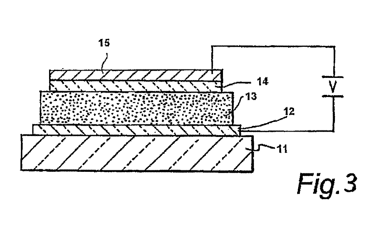
[0083]Referring to FIG. 3, a layer of PEDT / PSS (not shown) is deposited by spin-coating the formulation Baytron P® available from H C Starck of Leverkusen, Germany onto an indium tin oxide anode 12 supported on a glass substrate 11 (available from Applied Films, Colorado, USA). The PEDT / PSS layer is covered with a layer of a thin film of electroluminescent organic material 13. The organic material is a red-emissive co-polymer comprising repeat units of 9,9-dioctylfluoren-2,7-diyl; 2,1,3-benzothiadiazol-4,7-diyl; and 4,7-bis(2-thien-5-yl)-2,1,3-benzothiadiazole as disclosed in WO 01 / 49768. A composite layer 14 of BaF and Ca or Ba is co-deposited by electron beam co-evaporation, thermal co-evaporation or co-sputtering on organic layer 13. Capping layer 15 of aluminum is applied by electron beam evaporation, thermal evaporation or sputtering. Finally, the device is encapsulated using a metal enclosure available from Saes Getters SpA (not shown) that is glued to the substrate in order t...

example 2

[0084]The process described above was followed except that a full color display was formed according to the process described in EP 0880303 by forming wells for red, green and blue subpixels using standard lithographical techniques; inkjet printing PEDT / PSS into each subpixel well; and inkjet printing red, green and blue electroluminescent materials into wells for red, green and blue subpixels respectively.

[0085]Devices according to the invention provide both good electron injection into the organic layer(s) of the OLED due to the presence of both the low workfunction metal and electron injecting metal compound, and at the same time provides increased stability as compared to a bilayer of the low workfunction metal / metal compound as a result of the metal compound being bound in a matrix of the metal, and consequently being less prone to migration into the organic layers of the device.

example 3

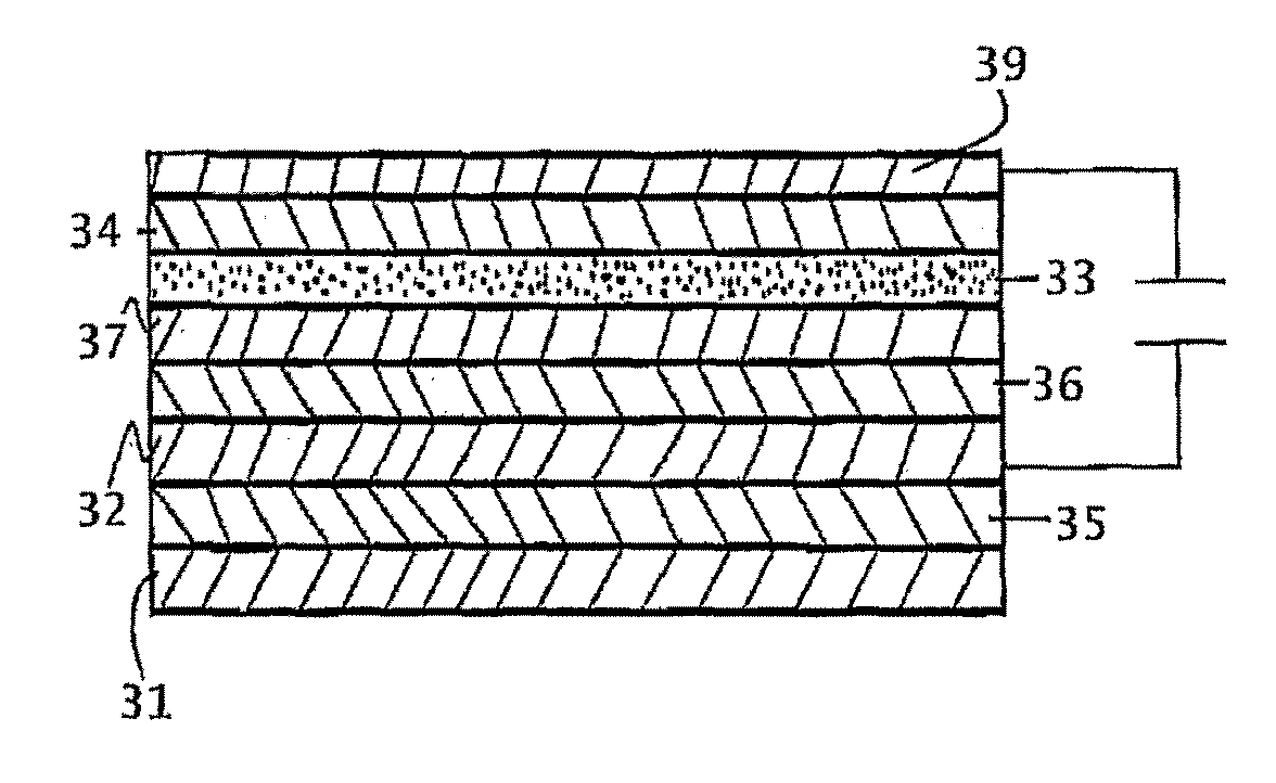
[0086]FIG. 4 shows in diagrammatic form a cross-sectional structure of a top emitting OLED according to the present invention. An anode material 32 such as ITO may be situated on a metal mirror 35 which is positioned over an active matrix back plane 31. Hole transporting material 36 is PEDT / PSS and is situated between anode 32 (ITO) and emissive layer 33. Optionally, a further intermediate layer 37 may be applied between the electron-injecting layer and the light emitting layer.

[0087]Composite combined cathode / buffer layer 34 is deposited over the light emitting layer 33 by electron beam coevaporation or thermal coevaporation. An indium tin oxide layer 39 is deposited by sputtering over the composite layer. Finally, a transparent encapsulation layer (not shown) is applied over the ITO layer so as to protect the device from ingress of oxygen and moisture. The encapsulation layer is generally a dielectric or polymer-dielectric composition.

Transparency Measurement

[0088]According to a f...


PUM


Abstract

An organic light emissive device comprising: a first electrode; a second electrode; and an organic light emissive region between the first and second electrodes comprising an organic light emissive material which has a peak emission wavelength, wherein at least one of the electrodes is transparent and comprises a composite of a charge injecting metal and another material which is codepositable with the charge injecting metal, the other material having a different refractive index to that of the charge injecting metal and wherein the other material has a lower degree of quenching at the peak emission wavelength than the charge injecting metal whereby quenching of excitons by the at least one electrode is reduced, the charge injecting metal comprising either a low work function metal having a work function of no more than 3.5 eV or a high work function metal having a work function of no less than 4.5 eV.

Description

CROSS-REFERENCE TO RELATED APPLICATION[0001]This is a continuation of U.S. patent application Ser. No. 11 / 659,930 filed Aug. 28, 2007 (now U.S. Pat. No. ______), which is the national phase of International Application No. PCT / GB2005 / 003135 filed Aug. 10, 2005, the entire respective disclosures of which are incorporated by reference in their entirety.BACKGROUND OF THE INVENTION[0002]1. Field of the Invention[0003]The invention relates to organic light emissive devices, to methods of making such devices and the use of cathodes therein.[0004]2. Related Technology[0005]Organic light emissive devices (OLEDs) generally comprise a cathode, an anode and an organic light emissive region between the cathode and the anode. Light emissive organic materials may comprise small molecular materials such as described in U.S. Pat. No. 4,539,507 or polymeric materials such as those described in PCT / WO90 / 13148. The cathode injects electrons into the light emissive region and the anode injects holes. T...

Claims


Application Information

Patent Timeline
Patent Type & Authority Applications(United States)
IPC IPC(8): H01L51/52H01L51/56
CPCH01L51/5206H01L2251/5315H01L51/5234H01L51/5221H10K50/81H10K50/828H10K2102/3026H10K50/805
Inventor SMITH, EUAN C.ROBERTS, MATTHEWYOUNG, WILLIAMFODEN, CLARE LOUISE
Owner CAMBRIDGE DISPLAY TECH LTD
Why Eureka
Try Eureka