Light emitting device

a technology of light-emitting devices and active layers, which is applied in the direction of semiconductor devices, lasers, semiconductor lasers, etc., can solve the problems of inability to obtain inability to efficiently excite constitutive layers, and inability to achieve light having a long wavelength of 500 nm. , to achieve the effect of increasing the absorption ratio of exciting light, high emission efficiency, and efficiently excitation constitutive layers

Inactive Publication Date: 2008-09-25
ROHM CO LTD
View PDF2 Cites 268 Cited by
  • Summary
  • Abstract
  • Description
  • Claims
  • Application Information

AI Technical Summary

Benefits of technology

[0009]According to this configuration, by incidence of induced emission light having a short wavelength from the laser on the nitride semiconductor light emitting element, it is possible to optically excite the quantum well layer forming the multiple-quantum well layer in the nitride semiconductor light emitting element. It is thus possible to generate light having a long wavelength from the nitride semiconductor light emitting element. Hence, because there is no need to electrically excite the quantum well layer, the nitride semiconductor light emitting element does not need to be provided with a light emitting diode structure. Accordingly, there is no need to form another layer (for example, a p-type semiconductor layer) that needs a treatment at such a high temperature that causes heat damage to the multiple-quantum well layer after the multiple-quantum well layer is formed. Consequently, the multiple-quantum well layer can emit light having a long wavelength at high efficiency.
[0010]In addition, because the group III nitride semiconductor laminating structure uses a non-polar plane or a semi-polar plane (that is, a plane other than c-plane) as the principal plane for crystal growth, it is possible to grow crystals in an extremely stable manner. Hence, in comparison with a case where c-plane is used as the principal plane for crystal growth, the crystalline property can be enhanced. It is thus possible to upgrade the quality of the group III nitride semiconductor laminating structure to consequently enhance emission efficiency.
[0011]Further, by using a group III nitride semiconductor having a non-polar plane or a semi-polar plane which is a different material from c-plane group III nitride semiconductor, it is possible to suppress separation of carriers due to spontaneous piezoelectric polarization in the quantum well layer. Therefore, emission efficiency is increased. Moreover, the current dependency of an emission wavelength is suppressed owing to the absence of the separation of carriers by the spontaneous piezoelectric polarization. It is thus possible to achieve a stable emission wavelength.
[0013]The laser may be a semiconductor laser made of a group III nitride semiconductor. Because the semiconductor laser merely needs to generate induced emission light having a short wavelength, even in a case where the laser is made of group III nitride semiconductor, the emission layer has durability against heat damage. There is no need for the nitride semiconductor light emitting element that is optically excited by the induced emission light from the semiconductor laser to have the light emitting diode structure. Accordingly, even an emission layer for a long wavelength can be manufactured without undergoing heat damage. It is thus possible to form a light emitting device capable of emitting light having a long wavelength at high emission efficiency using nitride semiconductor.
[0014]For example, the emission wavelength of the quantum well layer may be 500 nm to 650 nm, and the emission wavelength of the laser may be 300 nm to 450 nm. Light having a wavelength of 300 nm to 450 nm can efficiently excite constitutive layers (for example, a GaN layer and an InGaN layer) of the multiple-quantum well layer. In addition, by setting the emission wavelength of the quantum well layer to 500 nm to 650 nm, it is possible to obtain polarized light in a wavelength range showing green to red.
[0015]In addition, the multiple-quantum well layer may include not less than five quantum well layers. When configured in this manner, it is possible to increase an absorption ratio of exciting light.

Problems solved by technology

When an active layer (emission layer) having an emission wavelength of 500 nm or longer is formed from a group III nitride semiconductor, it is known that such an active layer is vulnerable to heat damage.
The active layer undergoes heat damage in this instance, and emission efficiency is impaired significantly.
It is therefore by no means easy to obtain light having a long wavelength of 500 nm or longer.

Method used


Image

  • Light emitting device
  • Light emitting device
  • Light emitting device

Examples


Embodiment Construction

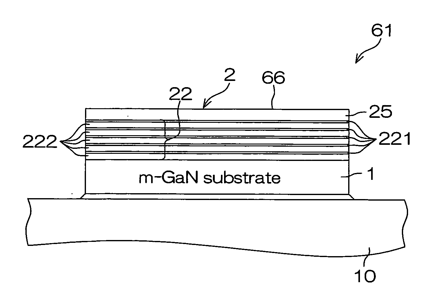
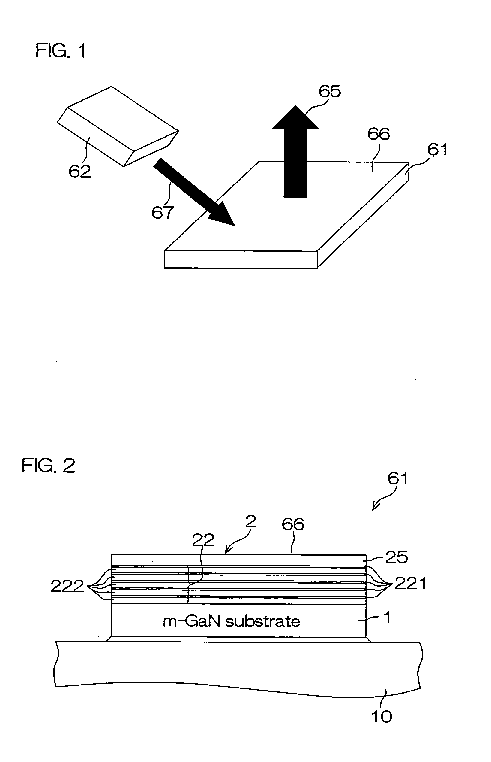
[0022]FIG. 1 is a schematic perspective view describing the configuration of a light emitting device according to one embodiment of the invention. The light emitting device includes a nitride semiconductor light emitting element 61 and a semiconductor laser 62.

[0023]The nitride semiconductor light emitting element 61 is made of a group III nitride semiconductor and generates light having a long wavelength of 500 nm or longer (for example, 532 nm). In this embodiment, the nitride semiconductor light emitting element 61 is configured to emit polarized light 65 to the exterior from a light extracting surface 66.

[0024]The semiconductor laser 62 is made of a group III nitride semiconductor, and generates a laser beam 67 (induced emission light) having a shorter wavelength (less than 450 nm, for example, 405 nm) than the emission wavelength of the nitride semiconductor light emitting element 61. To be more concrete, the semiconductor laser 62 is, for example, a known Fabry-Perot laser hav...


PUM


Abstract

A light emitting device includes a nitride semiconductor light emitting element provided with a group III nitride semiconductor laminating structure and a laser. The group III nitride semiconductor laminating structure has a non-polar plane or a semi-polar plane as a principal plane for crystal growth and includes a multiple-quantum well layer having a quantum well layer as an emission layer containing In and a barrier layer having a wider band gap than that of the quantum well layer. The laser generates induced emission light having a wavelength shorter than an emission wavelength of the quantum well layer and optically excites the quantum well layer in the nitride semiconductor light emitting element with the induced emission light.

Description

BACKGROUND OF THE INVENTION[0001]1. Field of the Invention[0002]The present invention relates to a light emitting device using a nitride semiconductor.[0003]2. Description of Related Art[0004]Of the group III-V semiconductors, semiconductors using nitrogen as group V elements are referred to as group III nitride semiconductors. Representative examples are aluminum nitride (AlN), gallium nitride (GaN), and indium nitride (InN). Generally, they are expressed as AlxInyGal-x-yN, where 0≦x≦1, 0≦y≦1, and 0≦x+y≦1.[0005]A manufacturing method of a nitride semiconductor was been known to grow a group III nitride semiconductor on a gallium nitride (GaN) substrate having the principal plane in the c-plane by metalorganic chemical vapor deposition (MOCVD). By adopting this method, it is possible to form a group III nitride semiconductor laminating structure having an n-type layer and a p-type layer to fabricate a light emitting device using this laminating structure.[0006]When an active layer (...

Claims


Application Information

Patent Timeline
Patent Type & Authority Applications(United States)
IPC IPC(8): H01S5/32H01L33/06H01L33/32
CPCB82Y20/00H01S5/041H01S5/183H01S2304/04H01S5/34333H01S2301/14H01S5/3202H01S5/32025
Inventor OKAMOTO, KUNIYOSHIOHTA, HIROAKI
Owner ROHM CO LTD
Why Eureka
Try Eureka