Dual work function buried gate-type transistor, method for forming the same, and electronic device including the same

a gate-type transistor and dual work function technology, applied in the field of transistors, can solve the problems of reducing gate resistance, high work function, and reducing channel impurity dose, and achieve the effect of improving gate-induced drain current properties and driving capability

Active Publication Date: 2015-12-03
SK HYNIX INC
View PDF5 Cites 238 Cited by
  • Summary
  • Abstract
  • Description
  • Claims
  • Application Information

AI Technical Summary

Benefits of technology

[0007]An embodiment is directed to a buried gate-type transistor that may improve gate-induced drain leakage (

Problems solved by technology

Metal gate electrodes of low resistance may reduce gate resistance.
Also, since the metal gate electrodes have a high work function, they may decrease channel impurity dose.
The high work function, however, has a problem in that gate-induced drain leakage (GIDL) is increased in an area where a metal gate electrode overlaps

Method used


Image

  • Dual work function buried gate-type transistor, method for forming the same, and electronic device including the same
  • Dual work function buried gate-type transistor, method for forming the same, and electronic device including the same
  • Dual work function buried gate-type transistor, method for forming the same, and electronic device including the same

Examples


first embodiment

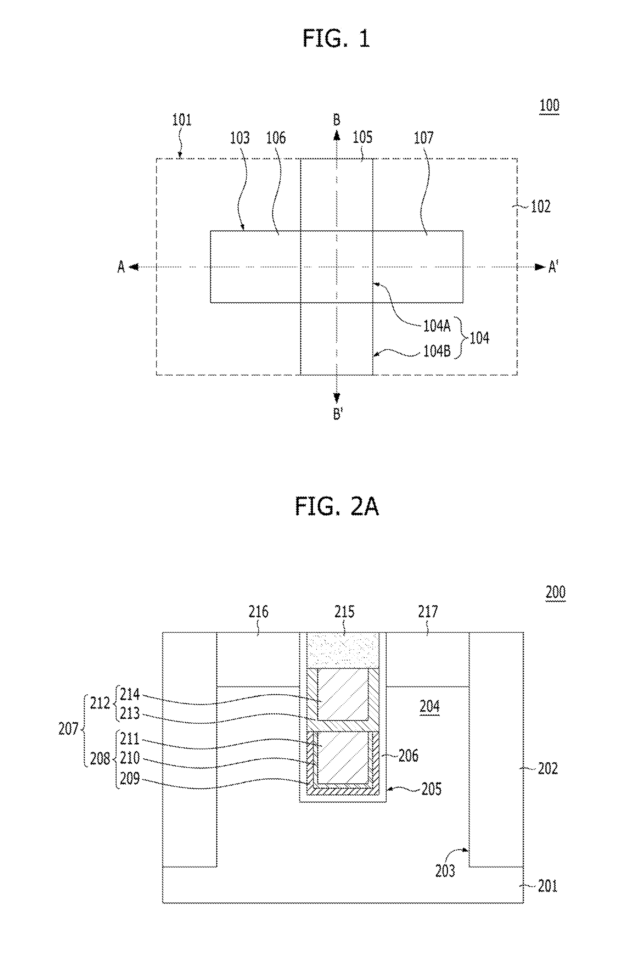
[0030]FIGS. 2A and 2B are cross-sectional views illustrating a transistor in accordance with a FIG. 2A is a cross-sectional view of the transistor 100 taken along a line A-A′ of FIG. 1. FIG. 2B is a cross-sectional view of the transistor 100 taken along a line B-B′ of FIG. 1.

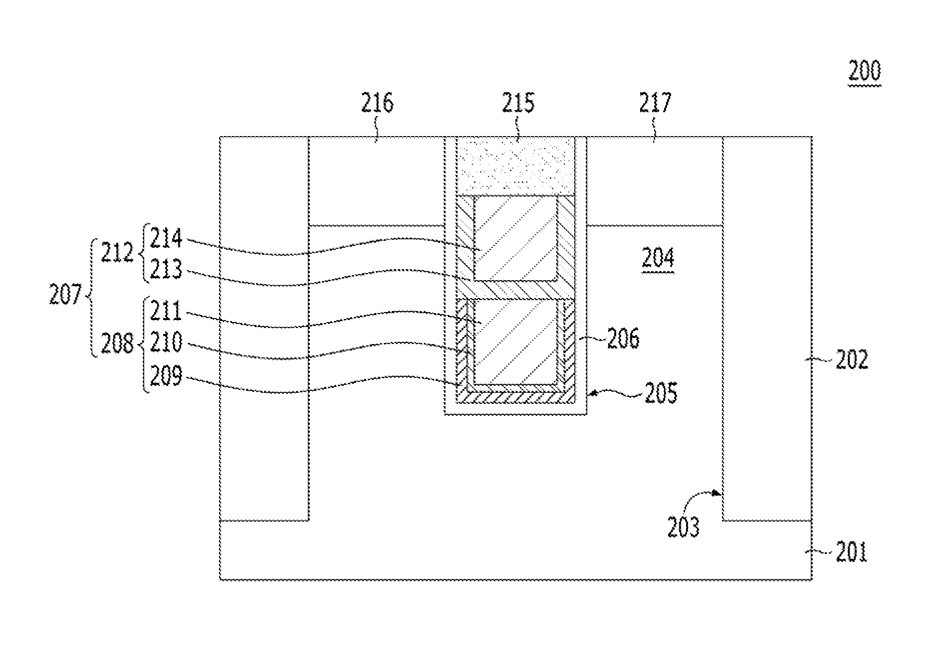
[0031]A transistor 200 is formed in a substrate 201. The substrate 201 includes a semiconductor substrate. The substrate 201 may include a silicon substrate or a Silicon On Insulator (SOI) substrate. An isolation layer 202 is formed in the substrate 201. The isolation layer 202 fills an isolation trench 203. The isolation layer 202 defines an active region 204 in the substrate 201. The active region 204 may have a shape of island.

[0032]A trench 205 having a predetermined depth is formed in the substrate 201. The trench 205 may have a shape of a line extending in one direction. The trench 205 may be formed across the active region 204 and the isolation layer 202. A depth of the trench 205 may be shallower than t...

second embodiment

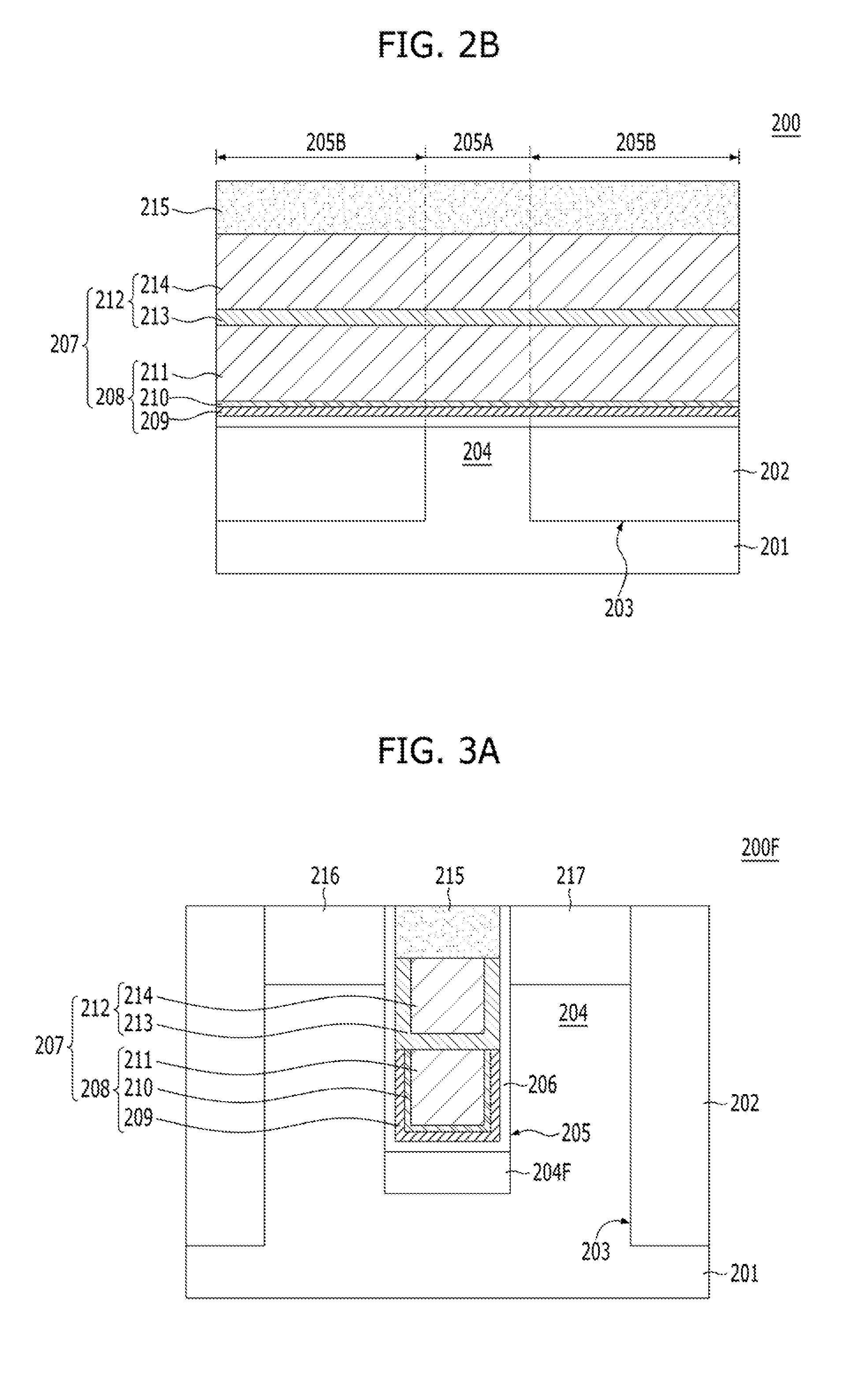
[0054]The transistor 200F in accordance with the second embodiment is referred to as a buried gate-type fin channel transistor.

[0055]According to the first embodiment and the second embodiment, sufficient threshold voltage characteristics are secured while controlling a doping concentration in a channel at a low level by applying the high work-function first barrier layer 209 to the lower buried portion 208 of the buried gate electrode 207. Herein, when titanium nitride containing aluminum is used as the first barrier layer 209, a dipole is formed based on the aluminum between the titanium nitride and the gate dielectric layer 206. With the dipole, high work function characteristics are obtained due to a change in energy band caused by interstitial oxygen.

[0056]Also, excellent gate-induced drain leakage (GIDL) characteristics are obtained by applying the low work-function second barrier layer 213 to the upper buried portion 212 of the buried gate electrode 207, while maintaining a d...


PUM


Abstract

A transistor includes: a source region and a drain region that are formed in a substrate to be spaced apart from each other; a trench formed in the substrate between the source region and the drain region; and a buried gate electrode inside the trench, wherein the buried gate electrode includes: a lower buried portion which includes a high work-function barrier layer including an aluminum-containing titanium nitride, and a first low-resistivity layer disposed over the high work-function barrier layer; and an upper buried portion which includes a low work-function barrier layer disposed over the lower buried portion and overlapping with the source region and the drain region, and a second low-resistivity layer disposed over the low work-function barrier layer.

Description

CROSS-REFERENCE TO RELATED APPLICATIONS[0001]The present application claims priority of Korean Patent Application No. 10-2014-0065279, filed on May 29, 2014, which is herein incorporated by reference in its entirety.BACKGROUND[0002]1. Field[0003]Exemplary embodiments relate to a transistor, and more particularly, to a dual work function buried gate-type transistor, a method for fabricating the transistor, and an electronic device including the transistor.[0004]2. Description of the Related Art[0005]Transistors employ metal gate electrodes as their gate electrodes. Metal gate electrodes of low resistance may reduce gate resistance. Also, since the metal gate electrodes have a high work function, they may decrease channel impurity dose. This may lead to reduced leakage current, thus improving performance of transistors.[0006]The high work function, however, has a problem in that gate-induced drain leakage (GIDL) is increased in an area where a metal gate electrode overlaps with an imp...

Claims


Application Information

Patent Timeline
IPC IPC(8): H01L29/423H01L29/78H01L29/51H01L29/66
CPCH01L29/4236H01L29/518H01L29/7813H01L29/66734H01L21/28088H01L29/4966H01L29/66621H01L29/66795H01L29/785H10B12/34H10B12/053H10B12/488H01L29/7809
Inventor KANG, DONG-KYUN
Owner SK HYNIX INC
Why Eureka
Try Eureka