Hydroxyl bond removal and film densification method for oxide films using microwave post treatment

a technology of oxide films and densification methods, which is applied in the direction of nuclear engineering, transportation and packaging, railway signalling, etc., can solve the problems of low density forming areas, increased feature depth to width, and insufficient conformal films of high aspect ratio features provided by traditional cvd techniques. , to achieve the effect of improving film properties, low thermal budget and increasing density

Active Publication Date: 2009-09-15
NOVELLUS SYSTEMS
View PDF76 Cites 256 Cited by
  • Summary
  • Abstract
  • Description
  • Claims
  • Application Information

AI Technical Summary

Benefits of technology

[0009]The present invention meets these needs by providing methods of forming dielectric films with increased density and improved film properties with low thermal budget. The methods involve exposing dielectric films to microwave radiation. According to various embodiments, the methods may be used to remove hydroxyl bonds, increase f...

Problems solved by technology

However, as design rules continue to shrink, the aspect ratios (depth to width) of features increase, and traditional CVD techniques can no longer provide adequately conformal films in these high aspect ratio features.
While ALD and PDL are useful to form conformal films, conventional ALD and PDL processes are apt to result in areas of low density forming in th...

Method used


Image

  • Hydroxyl bond removal and film densification method for oxide films using microwave post treatment
  • Hydroxyl bond removal and film densification method for oxide films using microwave post treatment
  • Hydroxyl bond removal and film densification method for oxide films using microwave post treatment

Examples


example 1

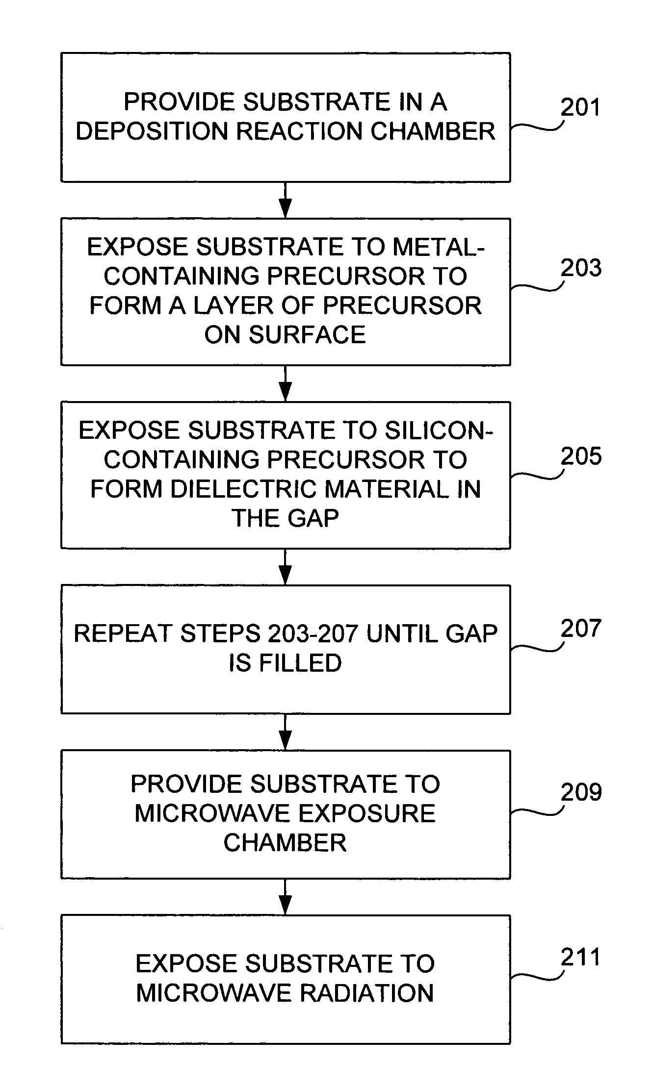
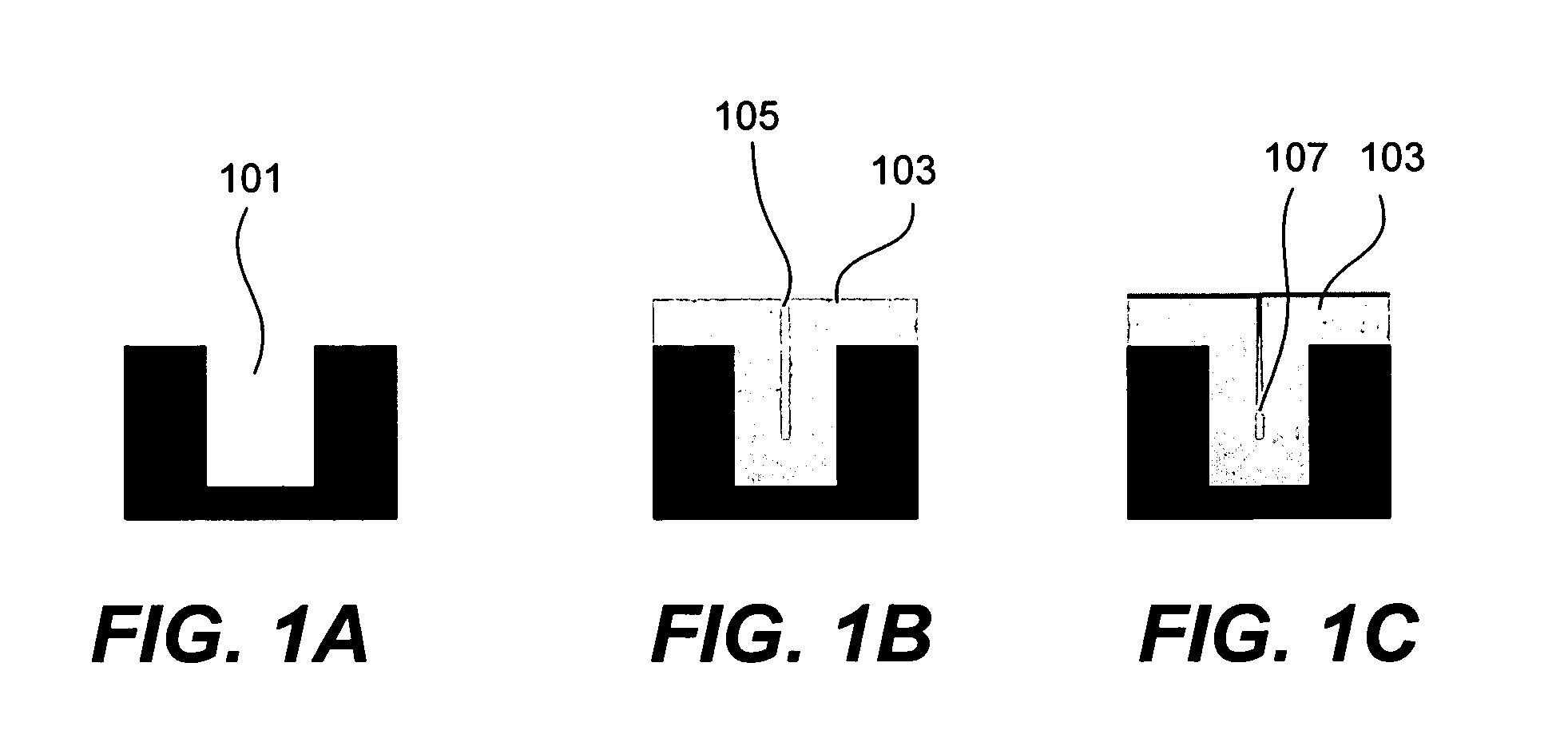
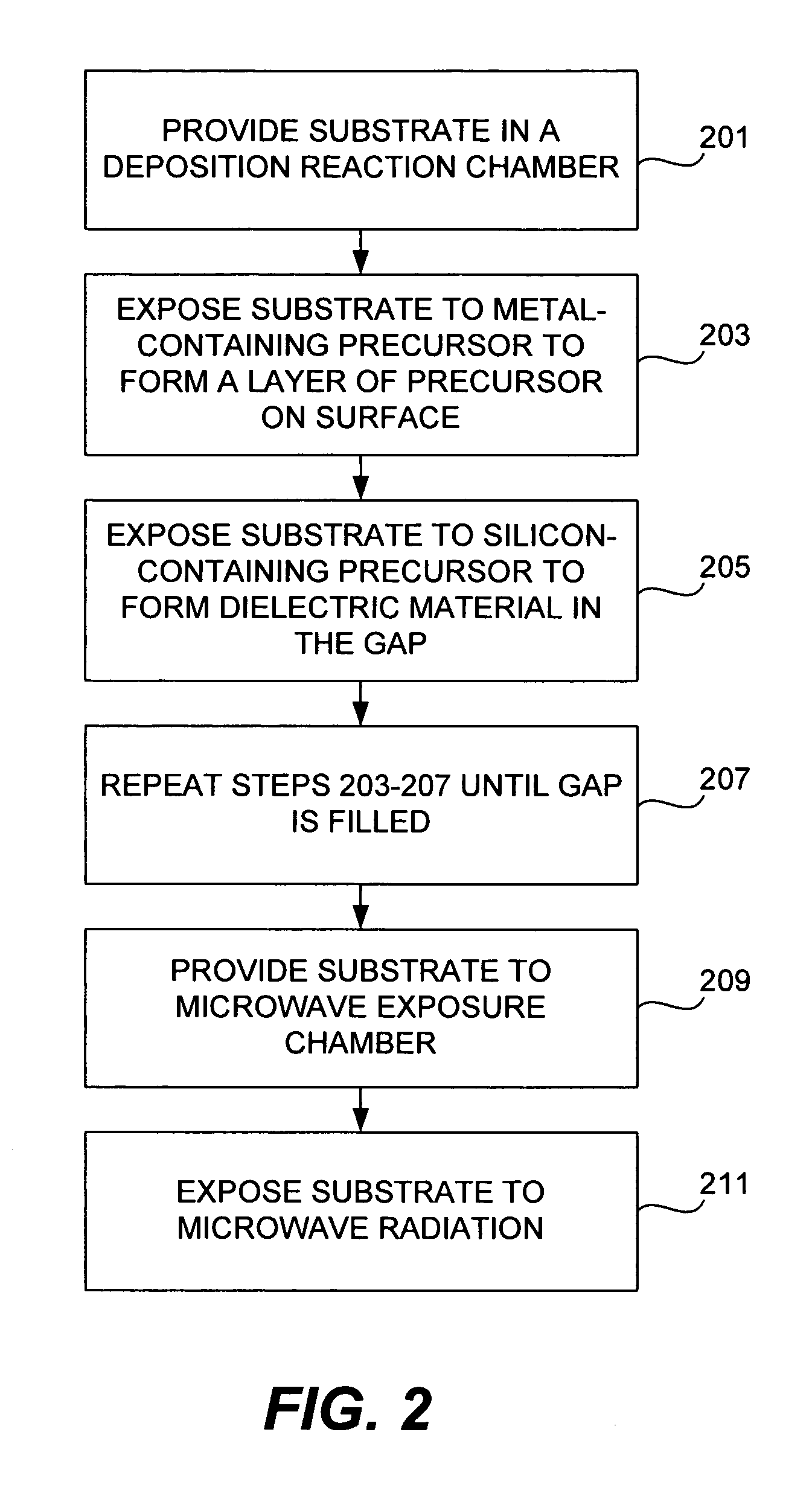
[0070]Dielectric film was deposited on a wafer by a pulsed deposition layer process using trimethylaluminum and tris(tert-pentoxy)silanol as the metal-containing and silicon-containing precursor gases, respectively. The deposited film was then exposed to microwave radiation at 2.45 GHz and 1200 W at atmospheric pressure. The overall substrate temperature did not exceed 400° C. during the microwave exposure. FTIR spectra of the film as deposited, and after 5 min and 60 minutes is shown in FIGS. 3A and 3B, and discussed above. As noted above, the hydroxyl bonds on the Si—OH groups were completely eliminated by 60 minutes of exposure. In addition, the dielectric constant was lowered from 7.0 to 4.0—indicating that the film was completely cured. Refraction index was lowered from 1.457 to 1.445. Film shrinkage was 5.0%.

[0071]Dielectric film was deposited on a wafer in the same manner as above, and subjected to thermal anneal at 400° C. until the peak at 3400 l / cm was reduced (indicating ...

example 2

[0072]Dielectric film was deposited on a wafer in the same manner as described in Example 1. The tensile stress of the deposited was measured as 93 MPa. The deposited film was then exposed to microwave radiation at 2.45 GHz and 1200 W at atmospheric pressure and air ambient for 40 minutes. Substrate temperature was less than or equal to 400° C. Tensile stress was 323 MPa after annealing.

[0073]Dielectric film was deposited on a wafer as described above. The wafer was then thermally annealed at 600° C. for 1 hour. After annealing the tensile stress was measured at 125 MPa—significantly lower than that achieved by microwave annealing.

Other Embodiments

[0074]This method applies to the deposition of silica (USG). However, this method may also be used for depositing doped silica films, such as fluorine-doped silicate glass (FSG), phosphosilicate glass (PSG), boro-phospho-silicate glass (BPSG), or carbon doped low-k materials.

[0075]Other deposition co-reactants, such as silanols with varyin...


PUM


Abstract

Methods of forming dielectric films with increased density and improved film properties are provided. The methods involve exposing dielectric films to microwave radiation. According to various embodiments, the methods may be used to remove hydroxyl bonds, increase film density, reduce or eliminate seams and voids, and optimize film properties such as dielectric constant, refractive index and stress for particular applications. In certain embodiments, the methods are used to form conformal films deposited by a technique such as PDL. The methods may be used in applications requiring low thermal budgets.

Description

FIELD OF THE INVENTION[0001]This invention pertains to methods for forming high density dielectric films. More specifically, the invention pertains to methods of treating deposited dielectric films with microwave radiation.BACKGROUND OF THE INVENTION[0002]Layers of dielectric film are used in several applications in sub-micron integrated circuit (IC) fabrication. Four such applications are shallow trench isolation (STI), premetal dielectric (PMD), inter-metal dielectric (IMD) and interlayer dielectric (ILD). All four of these layers require silicon dioxide films that fill features of various sizes and have uniform film thicknesses across the wafer.[0003]Chemical vapor deposition (CVD) has traditionally been the method of choice for depositing conformal silicon dioxide films. However, as design rules continue to shrink, the aspect ratios (depth to width) of features increase, and traditional CVD techniques can no longer provide adequately conformal films in these high aspect ratio fe...

Claims


Application Information

Patent Timeline
IPC IPC(8): H01L21/31H01L21/461
CPCH01L21/02145H01L21/02214H01L21/0228H01L21/02345H01L21/02359H01L21/76837H01L21/31604H01L21/76825H01L21/76826H01L21/76828H01L21/3105
Inventor CHO, SEON-MEEBARNES, MIKESCHULBERG, MICHELLEPAPASOULIOTIS, GEORGE D.
Owner NOVELLUS SYSTEMS
Why Eureka
Try Eureka