

Method for checking alignment accuracy of a thin film transistor
- Summary
- Abstract
- Description
- Claims
- Application Information
AI Technical Summary
Benefits of technology
Problems solved by technology
Method used
Image

Examples
Embodiment Construction
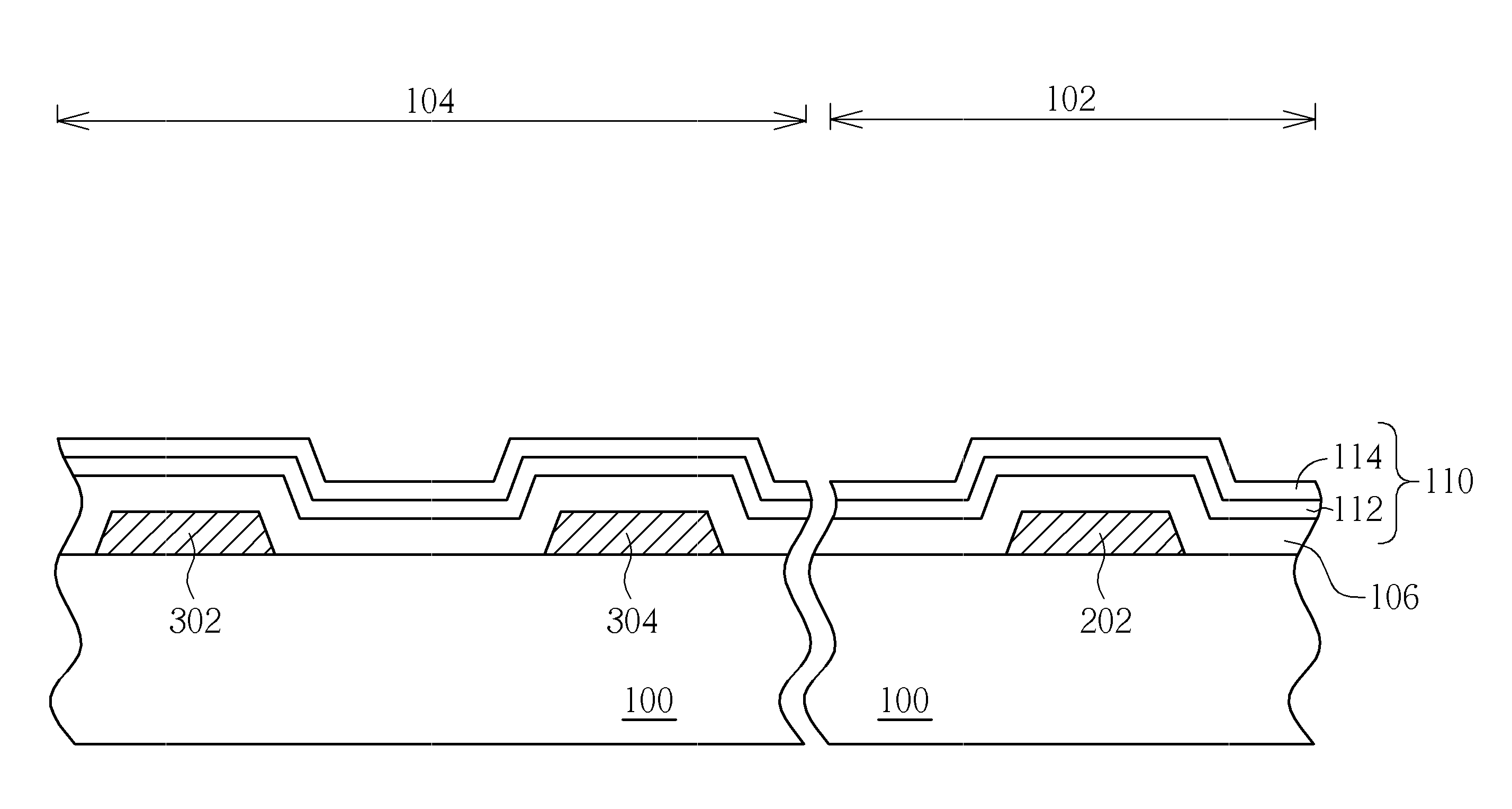
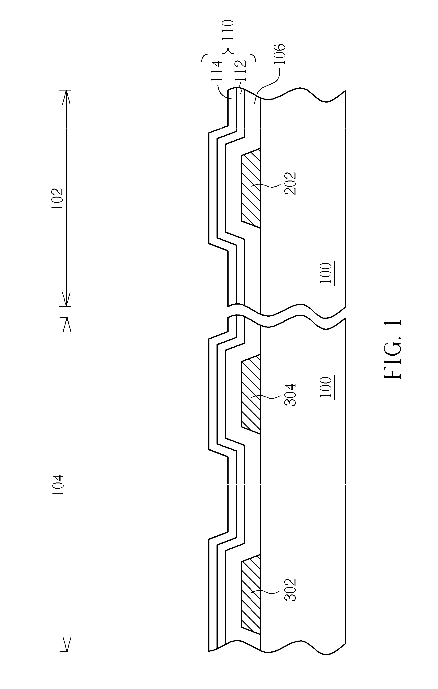
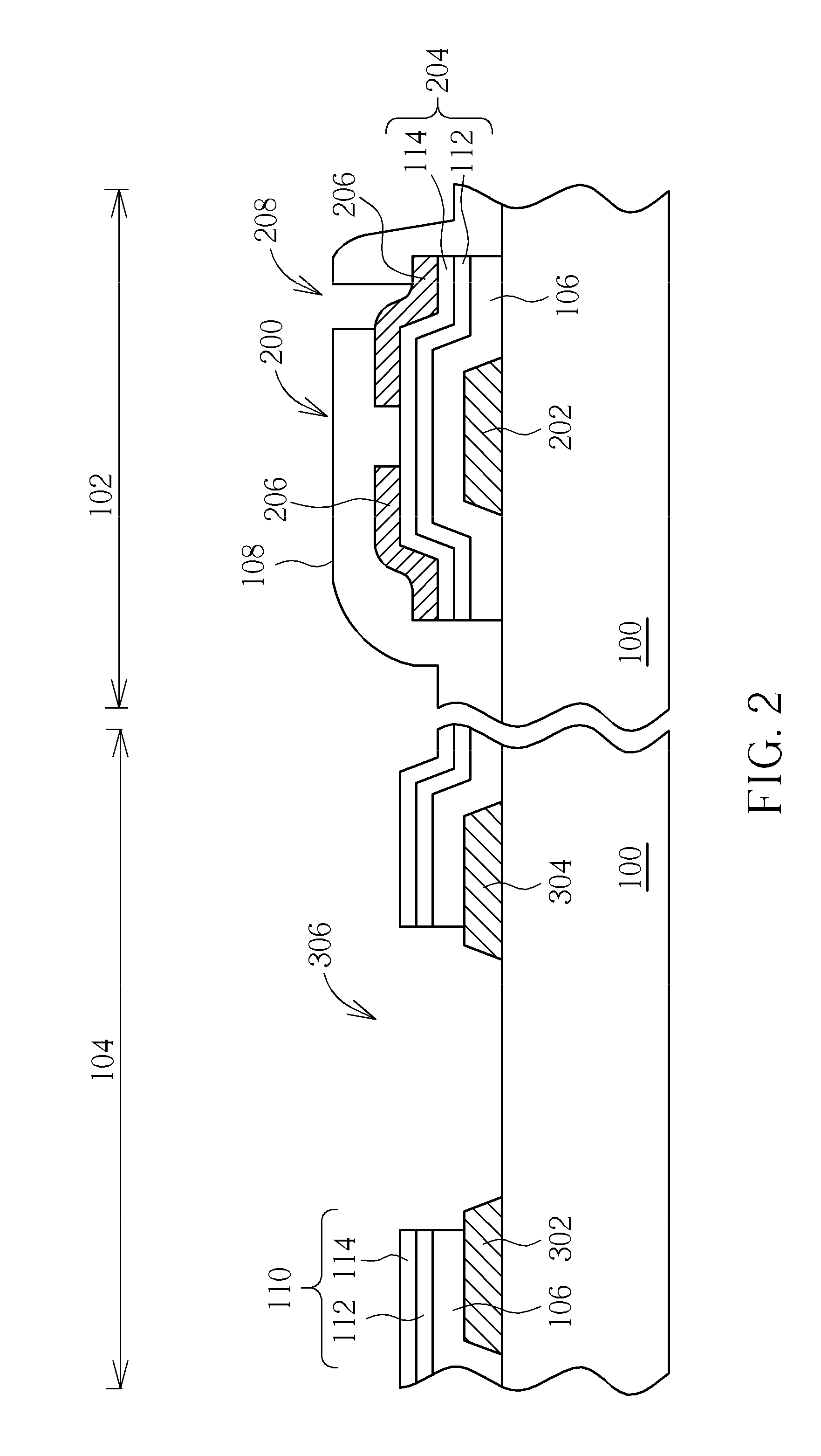
[0018]Please refer to FIGS. 1-4B, which are drawings illustrating a method for checking alignment accuracy of a TFT provided by a first preferred embodiment of the present invention, wherein FIGS. 4A-4B are schematic drawings illustrating a portion of the testing device provided by the preferred embodiment. As shown in FIG. 1, a substrate 100 having a pixel region 102 and a test region 104 defined thereon is provided. Then, a first conductive layer (not shown) is formed on the substrate 100 and followed by performing a first patterning process to the first conductive layer. Accordingly, a gate electrode 202 of a TFT is formed in the pixel region 102, and simultaneously a first terminal 302 and a second terminal 304 of a testing device are formed in the test region 104. It is noteworthy that the first terminal 302 and the second terminal 304 are electrically isolated from each other. Additionally, the first patterning process is well-known to those skilled in the art, therefore the d...
PUM
 Abstract
Description
Claims
Application Information