Semiconductor device and method for forming the same

Inactive Publication Date: 2012-01-19
SK HYNIX INC
View PDF1 Cites 2 Cited by
  • Summary
  • Abstract
  • Description
  • Claims
  • Application Information

AI Technical Summary

Benefits of technology

[0011]The present invention forms a gate oxidation layer using the oxidation rate difference without a mask process in order to minimize GIDL, which leads to improvement in the characteristics of a semiconductor device.

Problems solved by technology

However, one problem in the method for manufacturing a transistor with the recessed channel is that the etching selectivity is insignificant between the metal layer serving as the gate conductive layer and the high dielectric material layer serving as the gate oxidation layer.
The GIDL current significantly degrades a semiconductor device, especially in a DRAM device having a recessed channel.

Method used


Image

  • Semiconductor device and method for forming the same
  • Semiconductor device and method for forming the same
  • Semiconductor device and method for forming the same

Examples


Embodiment Construction

[0014]Exemplary embodiments of the present invention are described with reference to the accompanying drawings in detail.

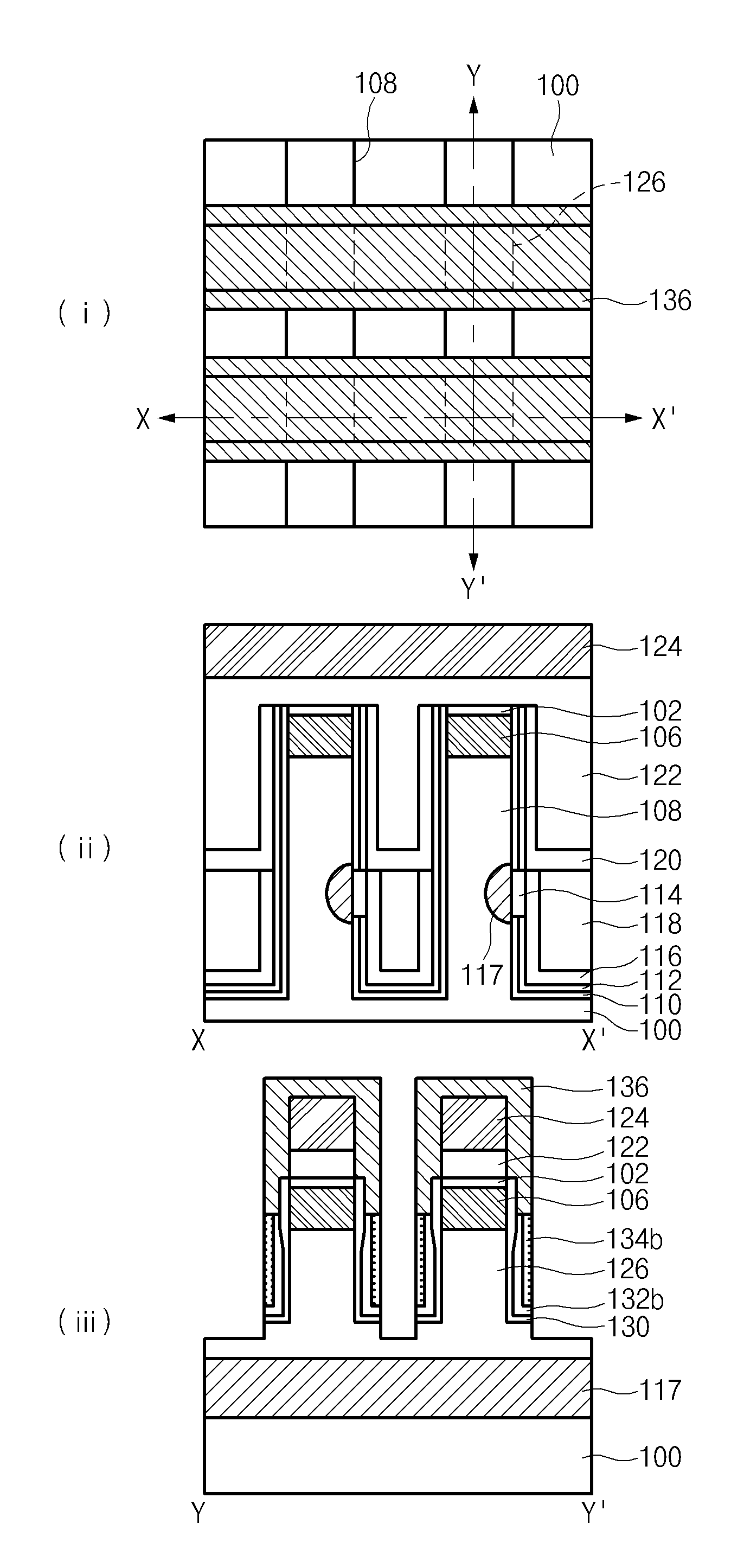
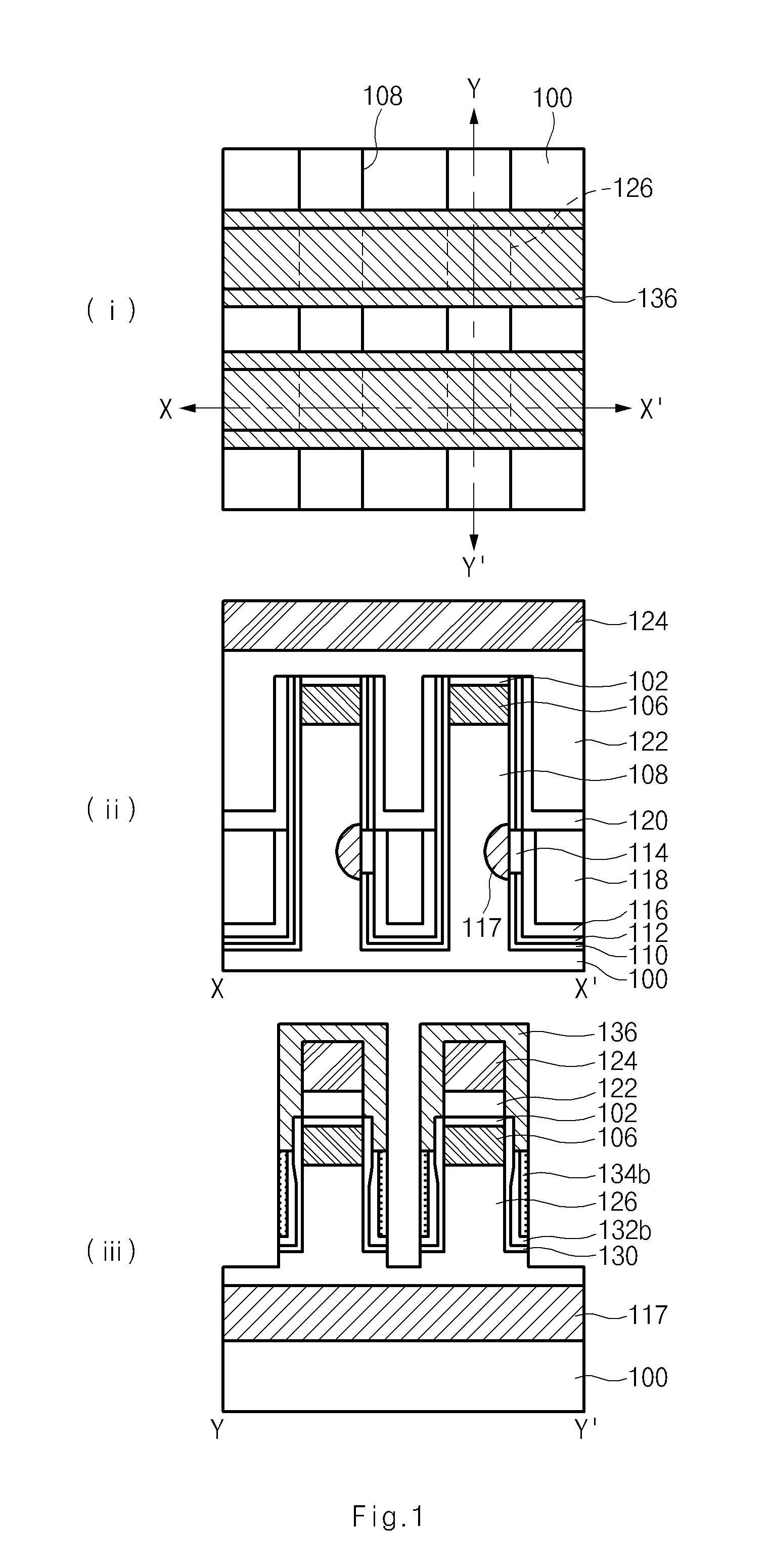
[0015]As shown in FIG. 1, it is preferred that a semiconductor device according to the present invention includes a vertical pillar 126 protruded from a semiconductor substrate 100; a first junction region 106 provided on the top of the vertical pillar 126; a second junction region 117 provided below the vertical pillar 126 to be separate from the first junction region 106; and a gate oxidation layer 130. In some embodiments, the vertical pillar 126 can be formed by etching the substrate 100 to the bottom of line pattern, so that the second junction region 117 can be located on a lower portion of the vertical pillar. The gate oxidation layer 130 is formed over a sidewall of the vertical pillar 126 and extending over a sidewall of first junction region 106. The thickness of the portion of gate oxidation layer 130 that is formed over the sidewall of the junction reg...


PUM


Abstract

The present invention relates to a semiconductor device and a method for forming the same. The semiconductor device includes: a vertical pillar protruded from a semiconductor substrate; a first junction region provided at an upper part of the vertical pillar; a second junction region provided in a lower part of the vertical pillar to be separated apart from the first junction region; and a gate oxidation layer in which a thickness thereof in a surface of the vertical pillar in which the first junction region is provided being thicker than that in a surface of the vertical pillar in which the first junction region is not provided. The present invention forms a gate oxidation layer using the oxidation rate difference without a mask process to minimize GIDL that leads to improvement in the characteristic of a semiconductor device.

Description

CROSS-REFERENCES TO RELATED APPLICATIONS[0001]The present application claims priority to Korean patent application number 10-2010-0067859, filed on Jul. 14, 2010, which is incorporated by reference in its entirety.BACKGROUND OF THE INVENTION[0002]The present invention relates to a semiconductor device and a method for forming the same, and more particularly, to a semiconductor device including a vertical gage and a method of forming the same.[0003]As semiconductor devices become highly integrated, the size of active regions are decreased. The channel length of a transistor on the active region is also decreased. As the channel length of transistors is reduced, the short channel effect and the source / drain punch-through phenomenon occur. The punch through phenomenon affects the electric field at a channel region of a transistor and causes the electric potential to significantly increased. For example, in an access MOS transistor employed in a memory cell of DRAM, when the short chann...

Claims


Application Information

Patent Timeline
IPC IPC(8): H01L29/78H01L21/336
CPCH01L27/10876H01L29/7827H01L29/66666H01L29/42368H10B12/053H10B12/395
Inventor RYU, SEONG WAN
Owner SK HYNIX INC
Why Eureka
Try Eureka