Method and device to reduce gate-induced drain leakage (GIDL) current in thin gate oxide MOSFETs

a thin gate oxide mosfet and drain current technology, applied in the direction of semiconductor devices, electrical apparatus, transistors, etc., can solve the problems of degrading affecting the current driving capability of these devices, and affecting the performance of these devices, so as to achieve the effect of reducing the gate induced drain curren

Inactive Publication Date: 2006-11-23
MOULI CHANDRA V +1
View PDF22 Cites 1 Cited by
  • Summary
  • Abstract
  • Description
  • Claims
  • Application Information

AI Technical Summary

Benefits of technology

[0008] The method of the present invention employs a non-orthogonal ion implant process by which the gate-oxide layer in the gate-drain overlap region of a FET device is selectively doped with fluorine or chlorine ions. The dosage of the ion implant is such that the ion concentration increases the ‘electrical’ gate oxide thickness near the gate-source / drain corners, thereby lowering the dielectric constant of the gate-oxide layer in the gate-drain overlap region without actual thickness growth to the ion doped gate-oxide layer. Since GIDL is exponentially dependent on the magnitude of the surface electrical field, even a slight reduction in the electrical field results in a dramatic reduction in GIDL. Accordingly, supplementing existing FET fabrication processes with the method of the preset invention, lowers the effective surface electrical field in the overlap region, and thereby minimizes GIDL in FET devices wherein the present invention is practiced.
[0010] In accordance with one aspect of the present invention, provided is a circuit structure comprising a semiconductor layer; an oxide layer formed on the semiconductor layer; a polysilicon layer formed on the oxide layer; a gate structure formed from the polysilicon layer, the gate structure having a defined leading edge; and an overlap region beneath the gate structure and adjacent the leading edge having a predetermined ion implant concentration, the predetermined implant concentration is sufficient to increase the electrical gate oxide thickness in the overlap region.
[0011] In accordance with another aspect of the present invention, provided is a method for fabricating a structure on a semiconductor layer comprising the steps of forming an oxide layer on a semiconductor layer; forming a polysilicon layer on the oxide layer; patterning the polysilicon layer into a gate structure having a defined leading edge, and to expose the oxide layer; and implanting ions into the oxide layer at an overlap region beneath the gate structure and adjacent the defined leading edge to a predetermined ion implant concentration which is sufficient to increase the electrical gate oxide thickness only in the overlap region without thickness growth of the oxide layer, the ions being implanted at a tilt angle non-orthogonal to the plane of the semiconductor layer.
[0012] In accordance with still another aspect of the present invention, provided is a method of reducing Gate Induced Drain Leakage (GIDL) current within Field Effect Transistors (FETs) comprising the steps of: forming on a semiconductor substrate a field effect transistor structure comprising a gate oxide layer, a gate electrode on the gate oxide layer and two source / drain regions formed within the semiconductor substrate; annealing the semiconductor substrate; implanting ions into the gate oxide layer beneath the gate electrode and adjacent the drain region, which defines an overlap region, to a predetermined ion implant concentration which is sufficient to increase electrical gate oxide thickness only in the overlap region, the ions being implanted at a tilt angle non-orthogonal to the plane of the semiconductor substrate; and completing the fabrication of the semiconductor substrate.
[0013] An object of the present invention is to provide a method of reducing gate induced drain leakage current by selectively increasing the electrical gate oxide thickness only in the gate / drain overlap region during the fabrication of integrated circuits.
[0014] Another object of the invention is to provide a manufacturable method for fabricating integrated circuits which will result in reduced gate induced drain leakage.

Problems solved by technology

In the fabrication of integrated circuits, as the sizes of semiconductor devices, such as state-of-the-art Metal Oxide Semiconductor Field Effect Transistors (MOSFETs), are scaled down, performance issues regarding the current driving capabilities of these devices exist.
However, it has been observed that as the gate oxide is made thinner, gate-induced drain leakage (GIDL) currents degrade the performance of these devices as the GIDL currents become a larger percentage of the total sub-threshold leakage current.
Unfortunately, it has been observed that by increasing the doping density in the channel and source / drain regions, the surface electric field also increases, resulting in more band bending and hence, even more GIDL current.
Thus, difficulties exist in providing a scaled down semiconductor device having a suitable balance between high current driving capability and low GIDL current.
However, having a thick gate oxide in the gate-source region increases source resistance, which in turn, reduces the current driving capability of the device.
However, having an increased material thickness of the oxide layer in the gate-drain region hampers current drives of the transistor and also cause increased stress in the active area near the overlap region due to volume expansion.

Method used


Image

  • Method and device to reduce gate-induced drain leakage (GIDL) current in thin gate oxide MOSFETs
  • Method and device to reduce gate-induced drain leakage (GIDL) current in thin gate oxide MOSFETs
  • Method and device to reduce gate-induced drain leakage (GIDL) current in thin gate oxide MOSFETs

Examples


Embodiment Construction

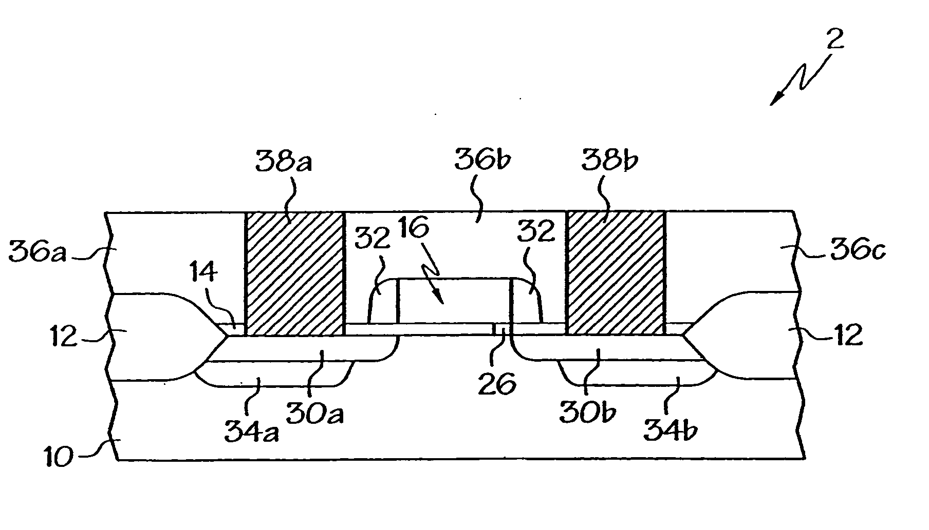
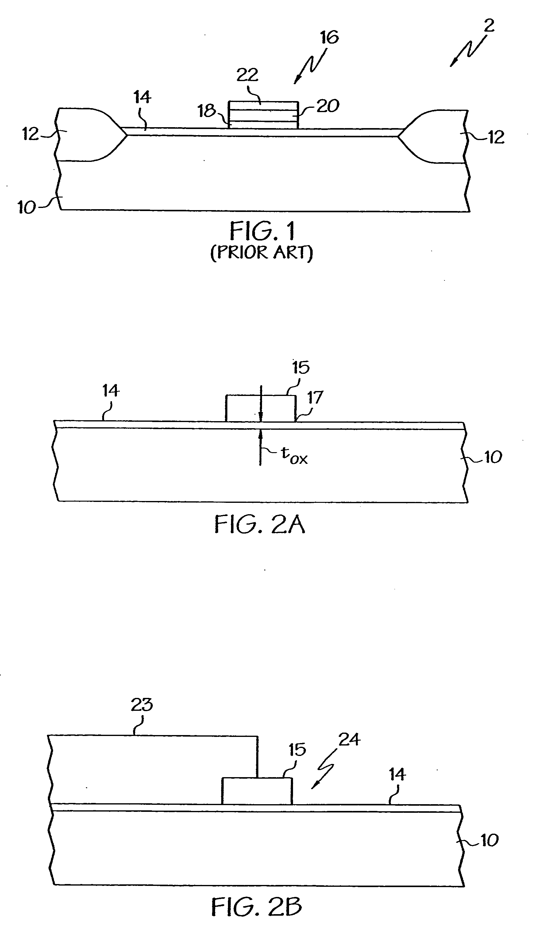
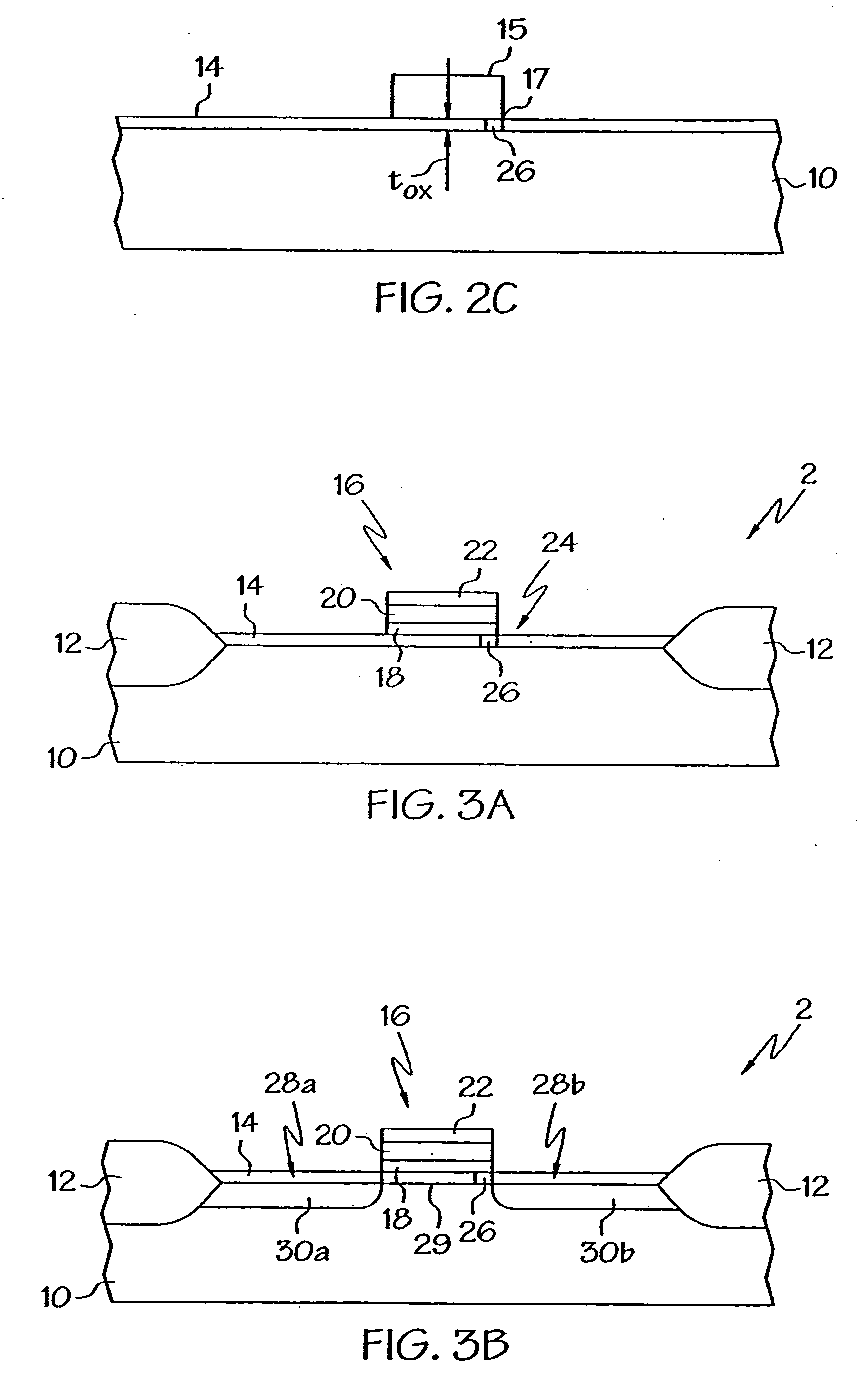
[0020]FIG. 1 is an illustration of a portion of a partially completed FET device 2, which can be formed by any known conventional method. As an example, and generally speaking, the FET device 2 is manufactured by the known local oxidation of silicon (LOCOS) process where portions of a semiconductor layer or substrate 10, through a lithographic mask, are oxidized to form field isolation regions 12. Field isolation regions 12 define active device regions and provide lateral isolation between adjacent devices also formed by the same mask in and on the surface of the substrate 10. For the sake of clarity, the field isolation regions 12 between devices have been only partially shown. Additionally, the formation of the lithographic mask is done by conventional lithography and etching techniques. It is to be appreciated that substrate 10 may be one or more semiconductor layers or structures, which includes active and operable portions of semiconductor devices, of various dopant concentrati...


PUM


Abstract

A process for the fabrication of an integrated circuit which provides a FET device having reduced GIDL current is described. A semiconductor substrate is provided wherein active regions are separated by an isolation region, and a gate oxide layer is form on the active regions. Gate electrodes are formed upon the gate oxide layer in the active regions. An angled, high dose, ion implant is performed to selectively dope the gate oxide layer beneath an edge of each gate electrode in a gate-drain overlap region, and the fabrication of the integrated circuit is completed.

Description

CROSS REFERENCE TO RELATED APPLICATIONS [0001] This application is a continuation of U.S. patent application Ser. No. 09 / 648,044 filed Aug. 25, 2000.TECHNICAL FIELD [0002] The invention relates to the fabrication of integrated circuit devices, and more particularly, to a method of reducing Gate Induced Drain Leakage (GIDL) current by selectively increasing electrical gate oxide thickness only in the gate / drain overlap region during the fabrication of integrated circuits. BACKGROUND OF THE INVENTION [0003] In the fabrication of integrated circuits, as the sizes of semiconductor devices, such as state-of-the-art Metal Oxide Semiconductor Field Effect Transistors (MOSFETs), are scaled down, performance issues regarding the current driving capabilities of these devices exist. Since the current driving capability is a function of both source resistance and gate oxide thickness, better performance in these devices is achievable through thinner gate oxide and spacer layers. However, it has...

Claims


Application Information

Patent Timeline
Patent Type & Authority Applications(United States)
IPC IPC(8): H01L21/8238H01L27/092H01L21/265H01L21/28H01L21/336H01L29/51H01L29/78
CPCH01L21/26506H01L21/26586H01L21/28176H01L29/66659H01L21/28194H01L29/512H01L29/518H01L21/28185H01L29/78H01L21/26513
Inventor MOULI, CHANDRA V.ROBERTS, CEREDIG
Owner MOULI CHANDRA V
Why Eureka
Try Eureka