

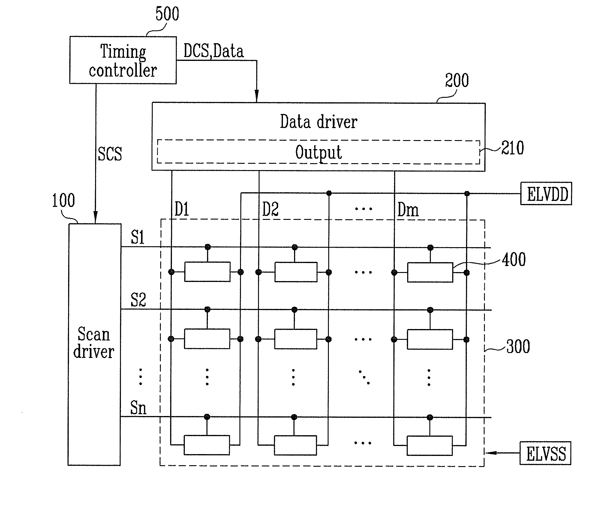
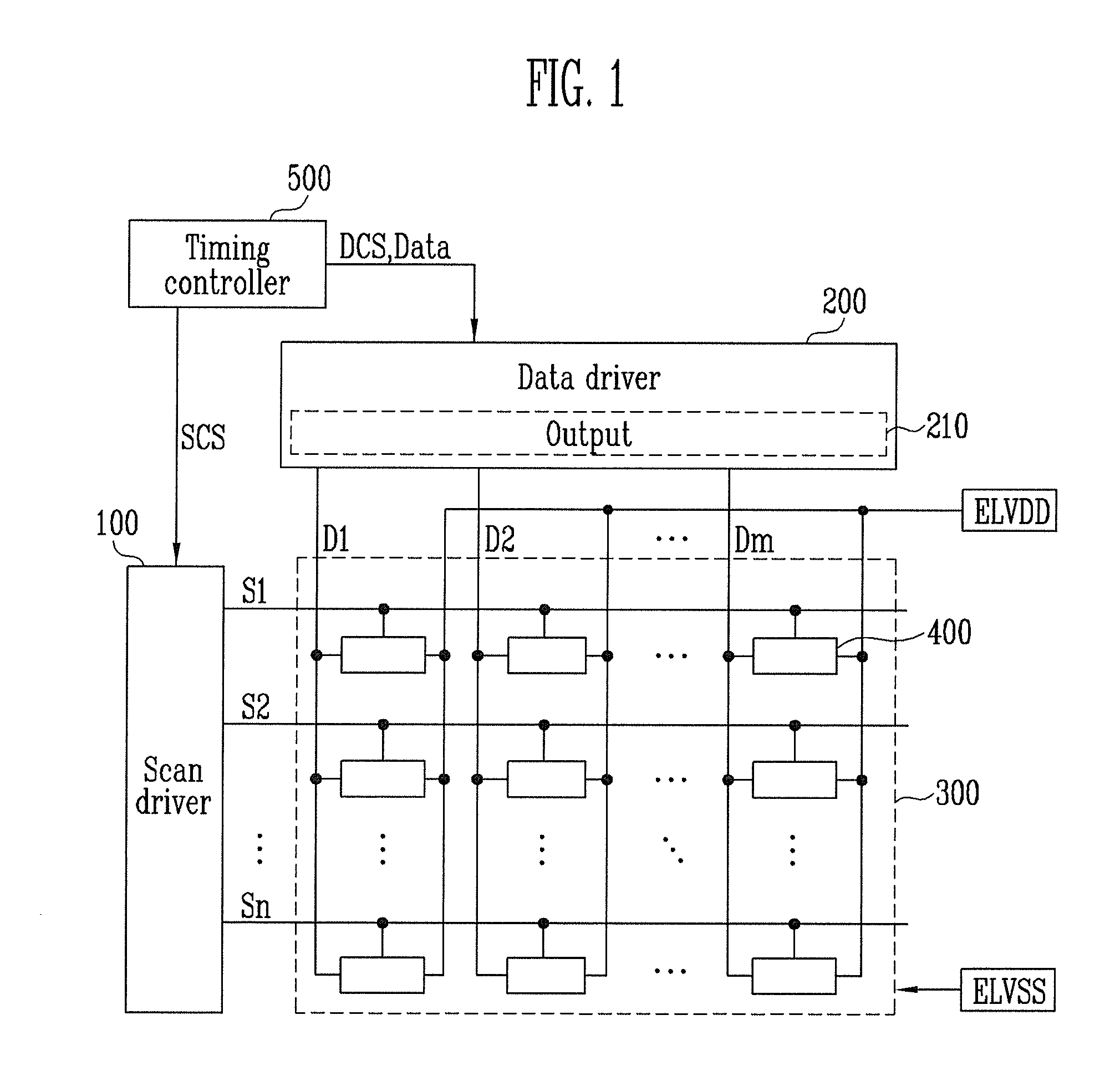
Data drive circuit of flat panel display and driving method thereof
a flat panel display and data drive technology, applied in the field of flat panel display and data drive circuit of flat panel display, can solve the problems of organic light emitting display screen deterioration, image quality degradation of stripes, etc., and achieve the effect of reducing channel output variations, preventing deterioration of screen quality due to vertical stripes
- Summary
- Abstract
- Description
- Claims
- Application Information
AI Technical Summary
Benefits of technology
Problems solved by technology
Method used
Image

Examples
first embodiment
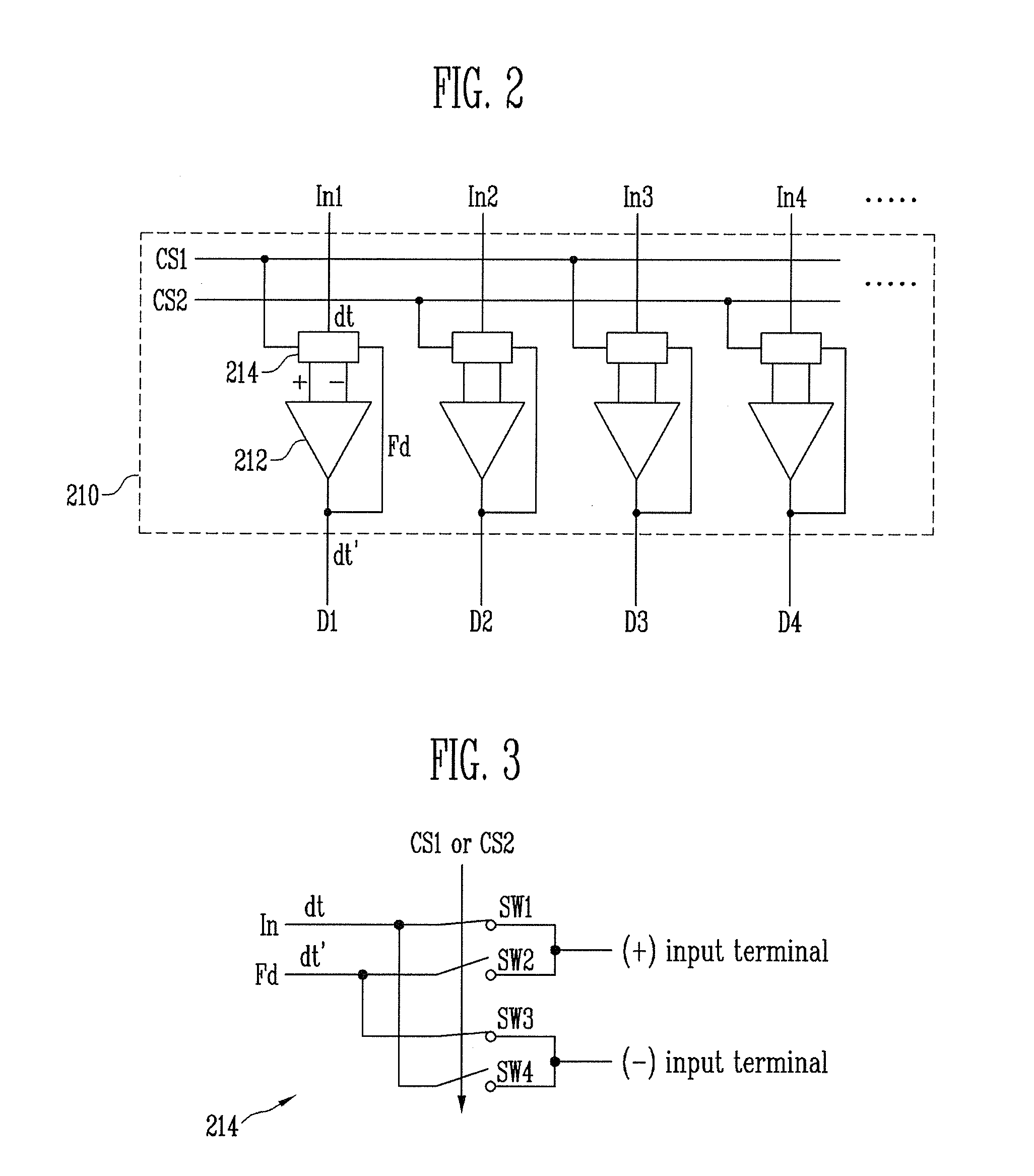
[0075]FIG. 4A is a view illustrating an offset calibration method according to the present invention. FIG. 4B is a timing diagram of signals for realizing the offset calibration method of the embodiment of FIG. 4A.
[0076]The offset calibration method according to the first embodiment of the present invention is a frame inversion method, and one-directional offsets are output in all frames as illustrated in FIG. 4A and offsets are sequentially changed (e.g., alternated) for respective frames in the method.
[0077]That is, a first data signal dt produced by the data driver is supplied to a positive input terminal of an amplifier in the n-th frame Frame N and the first data signal dt is input to a negative input terminal of the amplifier in the (n+1)-th frame Frame N+1.
[0078]Through changing the polarities of offsets in units of frames, a viewer may perceive an average of two frames (e.g., a calibrated offset value) to reduce or overcome deterioration of screen quality due to variations o...
second embodiment
[0082]FIG. 5A is a view illustrating an offset calibration method according to the present invention. FIG. 5B is a timing diagram of signals for realizing the offset calibration method of the embodiment of FIG. 5A.
[0083]The offset calibration method according to the second embodiment of the present invention is a column inversion method, and, as illustrated in FIG. 5A, the polarities of the offsets are opposite for columns of pixels and the offsets are sequentially changed (e.g., alternated) for frames.
[0084]That is, during the n-th frame Frame N, a first data signal dt produced by a data driver is supplied to a positive input terminal of an amplifier for a channel corresponding to an odd numbered column and a first data signal produced by the data driver for a channel corresponding to an even numbered column is supplied to a negative input terminal of the amplifier. They are input in an opposite way during the (n+1)-th frame Frame N+1.
[0085]In the offset calibration method, as illu...
third embodiment
[0089]FIG. 6A is a view illustrating an offset calibration method according to the present invention. FIG. 6B is a timing diagram of signals for realizing the offset calibration method of the embodiment of FIG. 6A.
[0090]The offset calibration method according to the third embodiment of the present invention is a line inversion method, and, as illustrated in FIG. 6A, deterioration of screen quality due to vertical channel variations is reduced or minimized by changing (e.g., alternating) the polarities of the offsets between adjacent horizontal lines, and offsets are sequentially changed (e.g., alternated) for respective frames.
[0091]That is, control signals are transited and applied during a plurality of horizontal time periods 1H of respective frames. In one embodiment of the present invention, the horizontal time periods 1H correspond to time periods during which scan signals are sequentially applied to scan lines.
[0092]In this case, during an n-th frame Frame N, first data signal...
PUM
 Abstract
Description
Claims
Application Information