
Circuit including first and second transistors coupled between an outpout terminal and a power supply

a technology of transistors and power supplies, applied in the direction of electric variable regulation, process and machine control, instruments, etc., can solve the problem that the output resistance rsub>out /sub>cannot be increased to be higher, and the limit of reducing the threshold voltage vt is difficult for engineers to determine the lower limit of operation voltage of analog circuits, etc. problems, to achieve the effect of reducing the influence of output voltage and reducing the variation of output curren

Active Publication Date: 2014-02-11
LONGITUDE LICENSING LTD
View PDF15 Cites 0 Cited by
  • Summary
  • Abstract
  • Description
  • Claims
  • Application Information

AI Technical Summary

Benefits of technology

The constant current source circuit helps control the output current to a constant level, which reduces the impact of changes in output voltage on the output current. This results in a constant output current in the low-voltage range.

Problems solved by technology

It becomes difficult for engineers to determine lower limits for operation voltages of analog circuits due to demands for reducing operation voltages of LSI (Large Scale Integration) circuits used in electronic devices having reduced power consumptions.
However, there is a limit in reducing the threshold voltage Vt due to an increase of a leak current.
In order to suppress variations of the output current I1 dependent upon the output voltage VOUT, it is necessary to increase the output resistance rOUT, whereas the circuitry of FIG. 13 suffers from a problem in that the output resistance rOUT cannot be increased to be higher than the drain resistance rDS1.

Method used


Image

  • Circuit including first and second transistors coupled between an outpout terminal and a power supply
  • Circuit including first and second transistors coupled between an outpout terminal and a power supply
  • Circuit including first and second transistors coupled between an outpout terminal and a power supply

Examples


first embodiment

1. First Embodiment

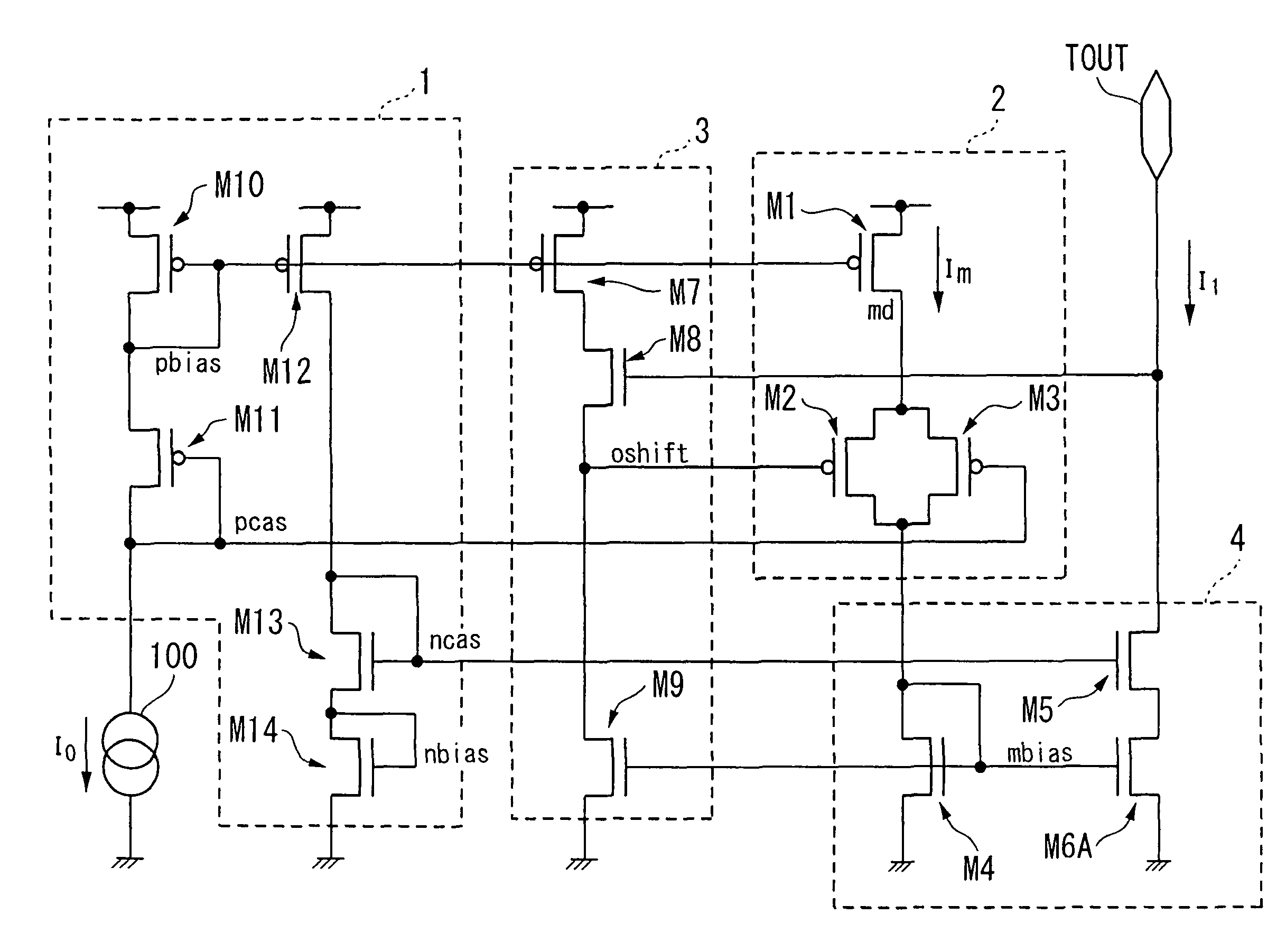
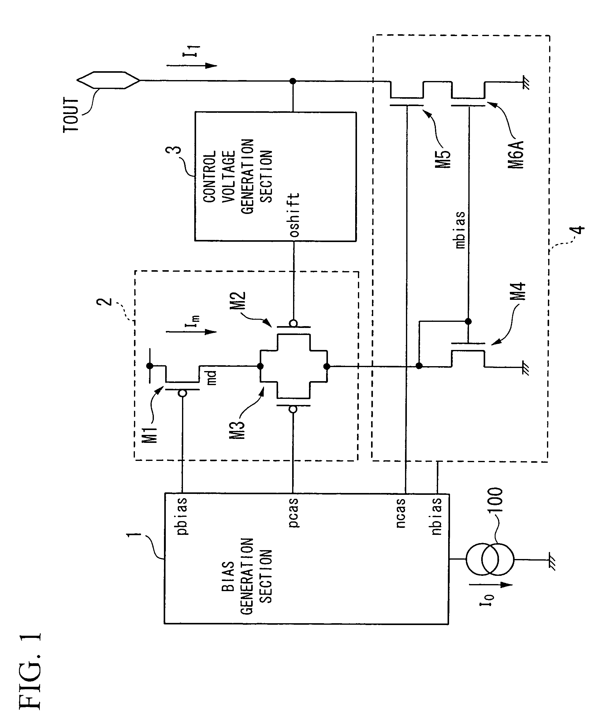
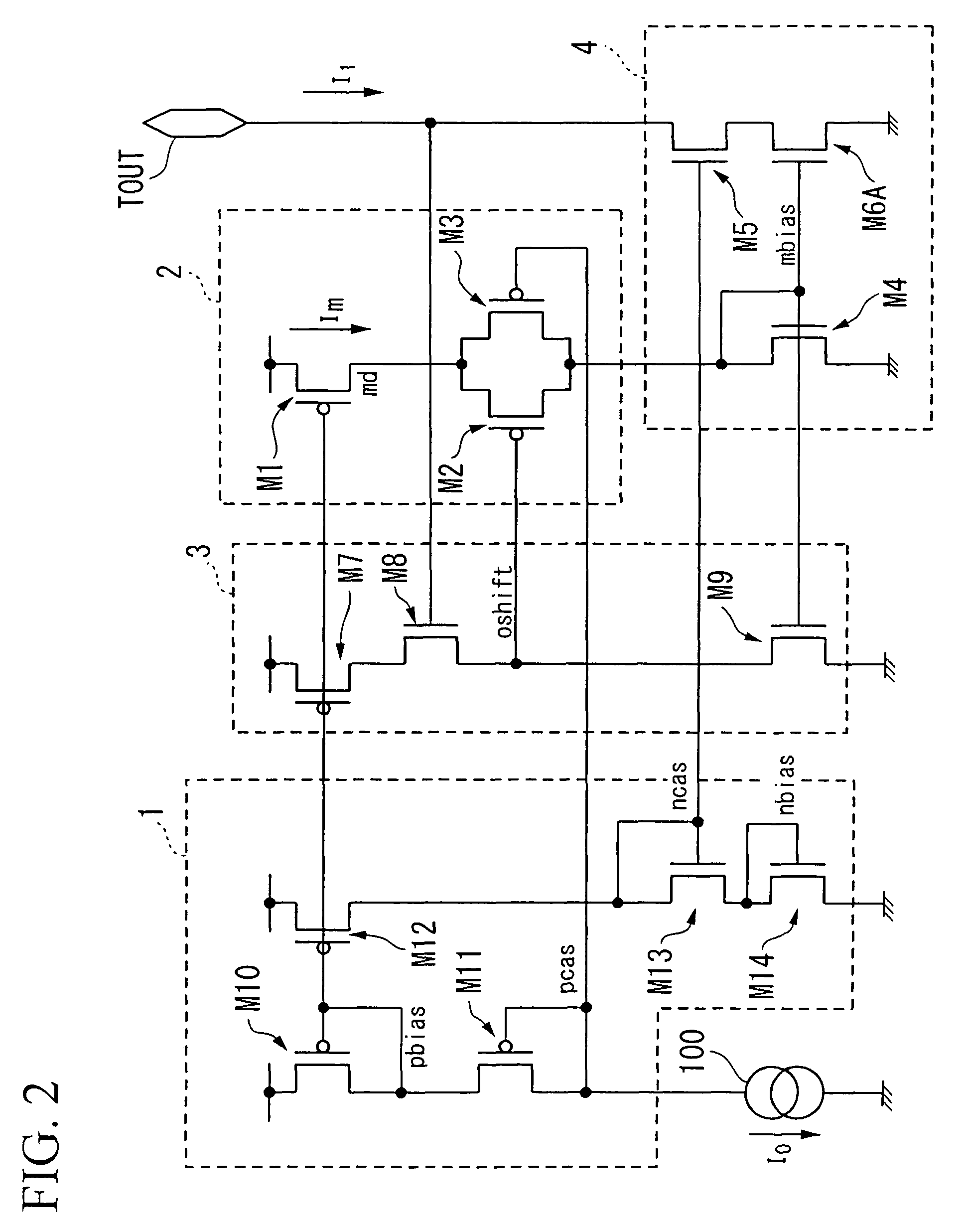
[0066]Referring now to FIG. 1, a constant current source circuit according to a first embodiment of the present invention includes a bias generation section 1, a reference current adjustment section 2, a control voltage generation section 3, and a current mirror section 4.

[0067]Based on a reference current I0 caused by a constant current source 100, the bias generation section 1 generates a first bias voltage pbias and a second bias voltage pcas for use in the reference current adjustment section 2 as well as a third bias voltage ncas for use in the current mirror section 4.

[0068]The output voltage of an output terminal TOUT is applied to the control voltage generation section 3. The control voltage generation section 3 generates a control voltage oshift, which is produced by shifting a prescribed voltage from the output voltage. It outputs the control voltage oshift to the reference current adjustment section 2.

[0069]The reference current adjustment section 2 is ...

second embodiment

2. Second Embodiment

[0106]Next, a constant current source circuit according to a second embodiment of the present invention will be described with reference to FIGS. 4 and 5. FIG. 5 is a circuit diagram showing the constitution of the constant current source circuit of the second embodiment.

[0107]Similar to the first embodiment, the constant current source circuit of the second embodiment is constituted of the bias generation section 1, the reference current adjustment section 2, the control voltage generation section 3, and the current mirror section 4.

[0108]In FIG. 5, parts identical to those of the first embodiment shown in FIG. 2 are designated by the same reference numerals; hence, only differences in the constitution and operation will be described with respect to the second embodiment.

[0109]Based on the reference current I0 created by the constant current source 100, the bias generation section 1 generates and outputs the first bias voltage pbias and the second bias voltage p...

third embodiment

3. Third Embodiment

[0117]Next, a constant current source circuit according to a third embodiment of the present invention will be described with reference to FIGS. 6 to 8. FIG. 6 is a circuit diagram showing the constitution of the constant current source circuit of the third embodiment. The third embodiment is designed to apply the reference current adjustment section 2 of the first embodiment to the low-voltage cascode current mirror circuit shown in FIG. 16.

[0118]The constant current source circuit of the third embodiment does not include the control voltage generation section 3 used in the first embodiment and is thus constituted of the bias generation section 1, the reference current adjustment section 2, and the current mirror section 4.

[0119]In FIG. 6, parts identical to those of the second embodiment shown in FIG. 5 are designated by the same reference numerals; hence, only differences in the constitution and operation will be described with reference to the third embodiment...


PUM


Abstract

A constant current source circuit is constituted of a control voltage generation section which detects the output voltage at the output terminal so as to generate a control voltage, a reference current adjustment section which adjust a reference current based on the control voltage, and a current mirror section which outputs the output current responsive to the adjusted reference current at the output terminal. This reduces variations of the output current due to variations of the output voltage; hence, the constant current source circuit can precisely operate in a low-voltage region.

Description

BACKGROUND OF THE INVENTION[0001]1. Field of the Invention[0002]The present invention relates to constant current source circuits that are used in integrated circuits and are produced by way of CMOS integrated circuit technologies.[0003]The present application claims priority on Japanese Patent Application No. 2007-258529, the content of which is incorporated herein by reference.[0004]2. Description of Related Art[0005]It becomes difficult for engineers to determine lower limits for operation voltages of analog circuits due to demands for reducing operation voltages of LSI (Large Scale Integration) circuits used in electronic devices having reduced power consumptions.[0006]This is greatly affected by the fact in which threshold voltages Vt for MOS (Metal Oxide Semiconductor) transistors will not be subjected to scaling relative to reductions of operation voltages.[0007]For example, when the minimum output voltage of a constant current source is to be reduced, it is necessary to redu...

Claims


Application Information

Patent Timeline
Patent Type & Authority Patents(United States)
IPC IPC(8): G05F3/20G05F3/16G05F1/00
CPCG05F3/262G05F3/16
Inventor IDE, AKIRA
Owner LONGITUDE LICENSING LTD
Learn More