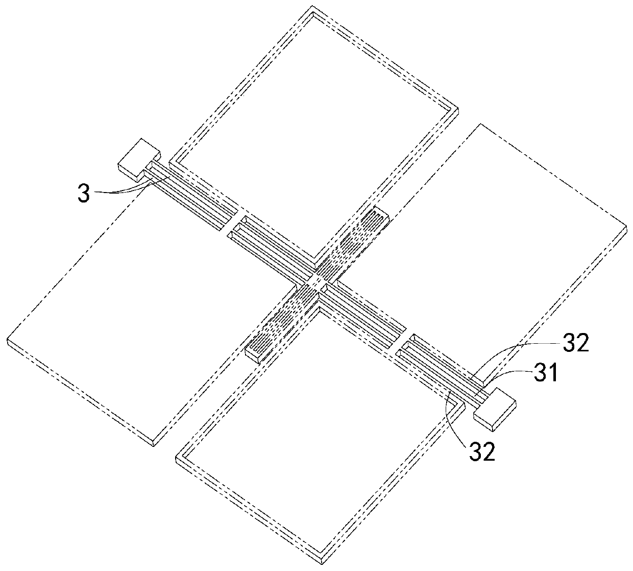
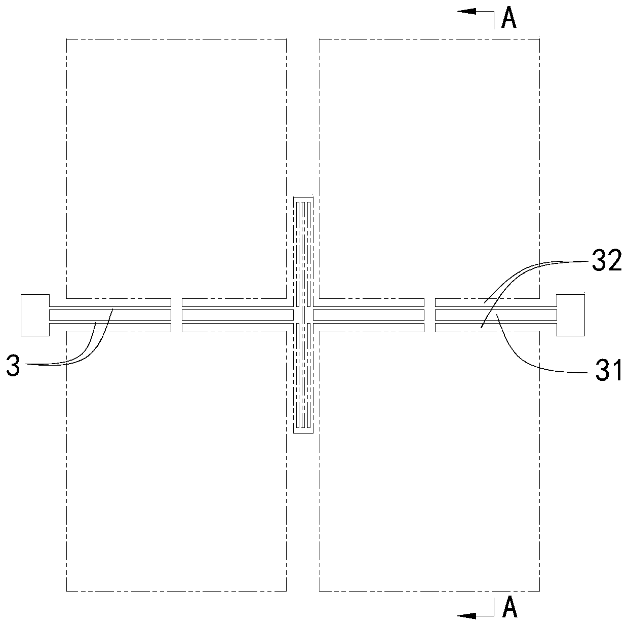
Silicon hollow beam, silicon micro-accelerometer based on silicon hollow beam and preparation method thereof

An accelerometer, hollow technology, used in the measurement of acceleration, velocity/acceleration/shock measurement, instruments, etc., can solve the problem of large bending modal interference of support beams, temperature characteristics and robustness limitations, poor anti-modal interference capabilities, etc. problem, to achieve the effect of improving anti-interference ability, low cost and high processing quality

Active Publication Date: 2020-07-17
NAT UNIV OF DEFENSE TECH
View PDF13 Cites 0 Cited by
  • Summary
  • Abstract
  • Description
  • Claims
  • Application Information

AI Technical Summary

Problems solved by technology

However, the ability to resist modal interference is poor, the noise is large, and the temperature characteristics and robustness are limited by its own structure.
[0004] Chinese patent documents with patent application numbers 201410825011.3 and 201410606833.2 disclose two types of micro-machined accelerometers, but the micro-accelerometers in the two schemes are single support beam structures, and there is a problem that the bending mode of the support beam is greatly disturbed; and the two The solutions are all prepared by wet etching process, which has problems such as large device area, low yield and high processing cost.

Method used


Image

  • Silicon hollow beam, silicon micro-accelerometer based on silicon hollow beam and preparation method thereof
  • Silicon hollow beam, silicon micro-accelerometer based on silicon hollow beam and preparation method thereof
  • Silicon hollow beam, silicon micro-accelerometer based on silicon hollow beam and preparation method thereof

Examples


preparation example Construction

[0067] Such as Figure 8 and Figure 9As shown, the basic steps of the preparation method of the silicon micro-accelerometer based on the silicon hollow beam in this embodiment include: using dry etching to process the prepared silicon substrate, bonding the silicon substrate and a piece of SOI silicon wafer by low stress bonding, The micro-accelerometer is obtained by preparing a silicon-sensitive structure by dry etching, and its specific implementation steps include:

[0068] a) Prepare the first SOI wafer as a silicon substrate such as Figure 8 Shown in (a); In the present embodiment, the thickness of the device layer of the SOI silicon wafer is 6 microns;

[0069] b) The device layer of the silicon base is dry etched for the first time to form a gap between the silicon substrate 1 and the silicon sensitive structure 2; in this embodiment, the first dry etching of the silicon base is 2 microns, and the formed gap is as follows Figure 8 as shown in (b);

[0070] c) On...


PUM


Abstract

The invention discloses a silicon hollow beam, a silicon microaccelerometer based on the silicon hollow beam, and a preparation method thereof. The silicon hollow beam comprises a beam body produced by performing dry etching on SOI silicon chips, and the cross section of the beam body is hollow. The microaccelerometer comprises a silicon sensitive structure and a silicon substrate, which are connected into one body. The silicon sensitive structure comprises a support beam and a sensitive mass block assembly. The cross section of the support beam is the said silicon hollow beam, and the sensitive mass block assembly is fixed to a mooring anchor through the support beam. The preparation method comprises the steps of adopting the silicon sensitive structure prepared by dry etching; bonding the silicon sensitive structure and the silicon substrate having a capacitance plate assembly and a lead wire electrode by adopting silicon-silicon low stress bonding, and obtaining the microaccelerometer. The invention is advantageous in that anti-interference capability is strong, device area is small, yield rate is high, cost is low, stability is high, processing quality is high, processing robustness is good, and application scope is wide.

Description

technical field [0001] The invention relates to silicon microsensor technology, in particular to a silicon hollow beam, a silicon micro accelerometer based on the silicon hollow beam and a preparation method thereof. Background technique [0002] Accelerometers are mainly used to measure the motion parameters of moving objects relative to inertial space. Compared with traditional acceleration, MEMS micro-accelerometer technology has the characteristics of small size, low power consumption, and easy batch processing, so it quickly becomes a research hotspot, and its performance is constantly improving, and it is widely used in military and civilian fields. [0003] At present, foreign uniaxial micro-accelerometer products have matured and been widely used. Domestic research and development of uniaxial micro-accelerometers are also increasing, and some laboratories have developed high-performance engineering. However, how to manufacture a single-axis micro-accelerometer with ...

Claims


Application Information

Patent Timeline
Patent Type & Authority Patents(China)
IPC IPC(8): G01P15/125
CPCG01P15/125
Inventor 肖定邦吴学忠侯占强周剑卓明苗桐侨李青松欧芬兰
Owner NAT UNIV OF DEFENSE TECH
Why Eureka
Try Eureka