Detection device, electronic device, and robot
a detection device and electronic technology, applied in the direction of force measurement, force measurement, instruments, etc., can solve the problems of inability to measure the force of the in-plane direction of the external pressure applied to the measurement surface. achieve the effect of high precision
- Summary
- Abstract
- Description
- Claims
- Application Information
AI Technical Summary
Benefits of technology
Problems solved by technology
Method used
Image
Examples
first embodiment
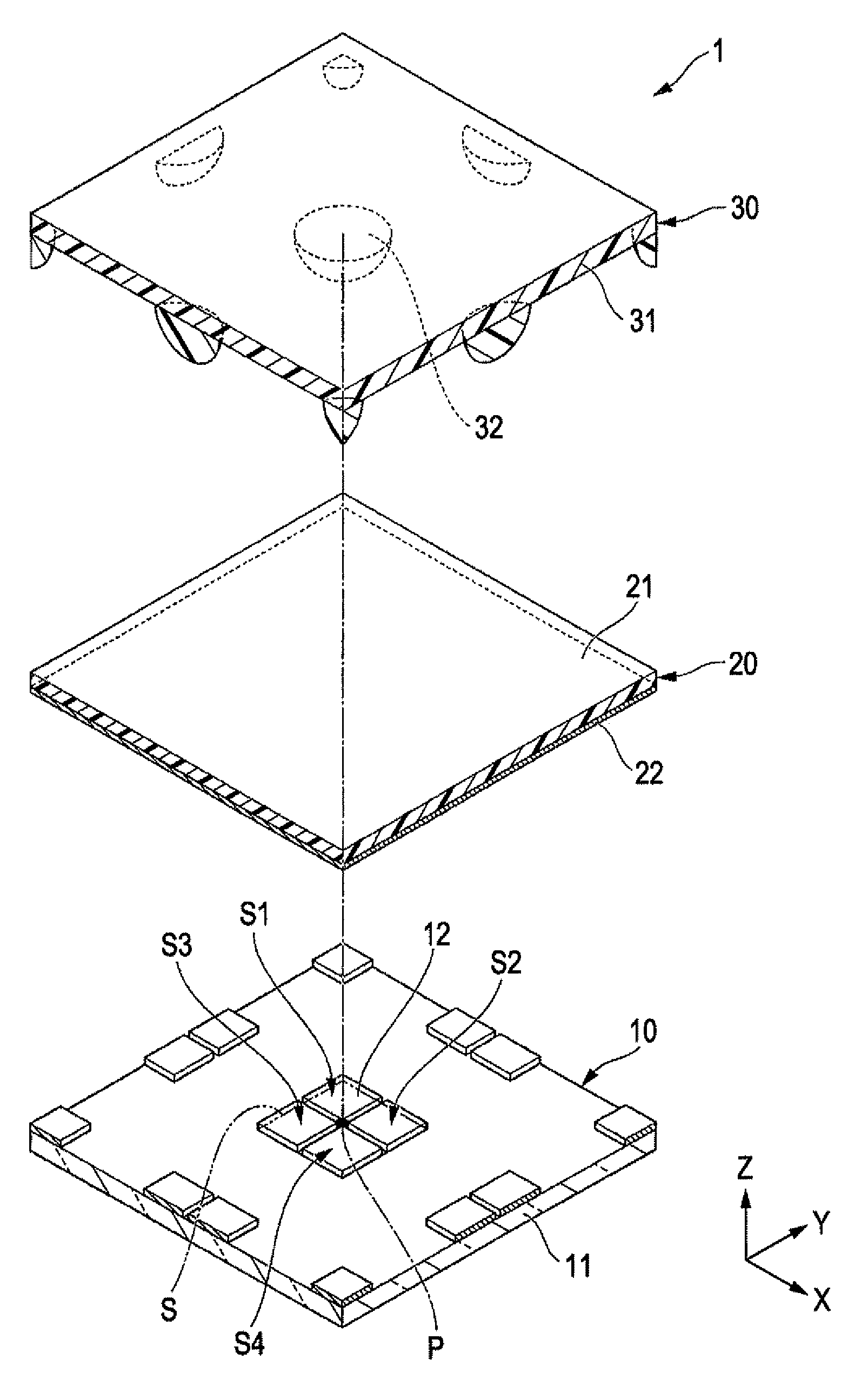
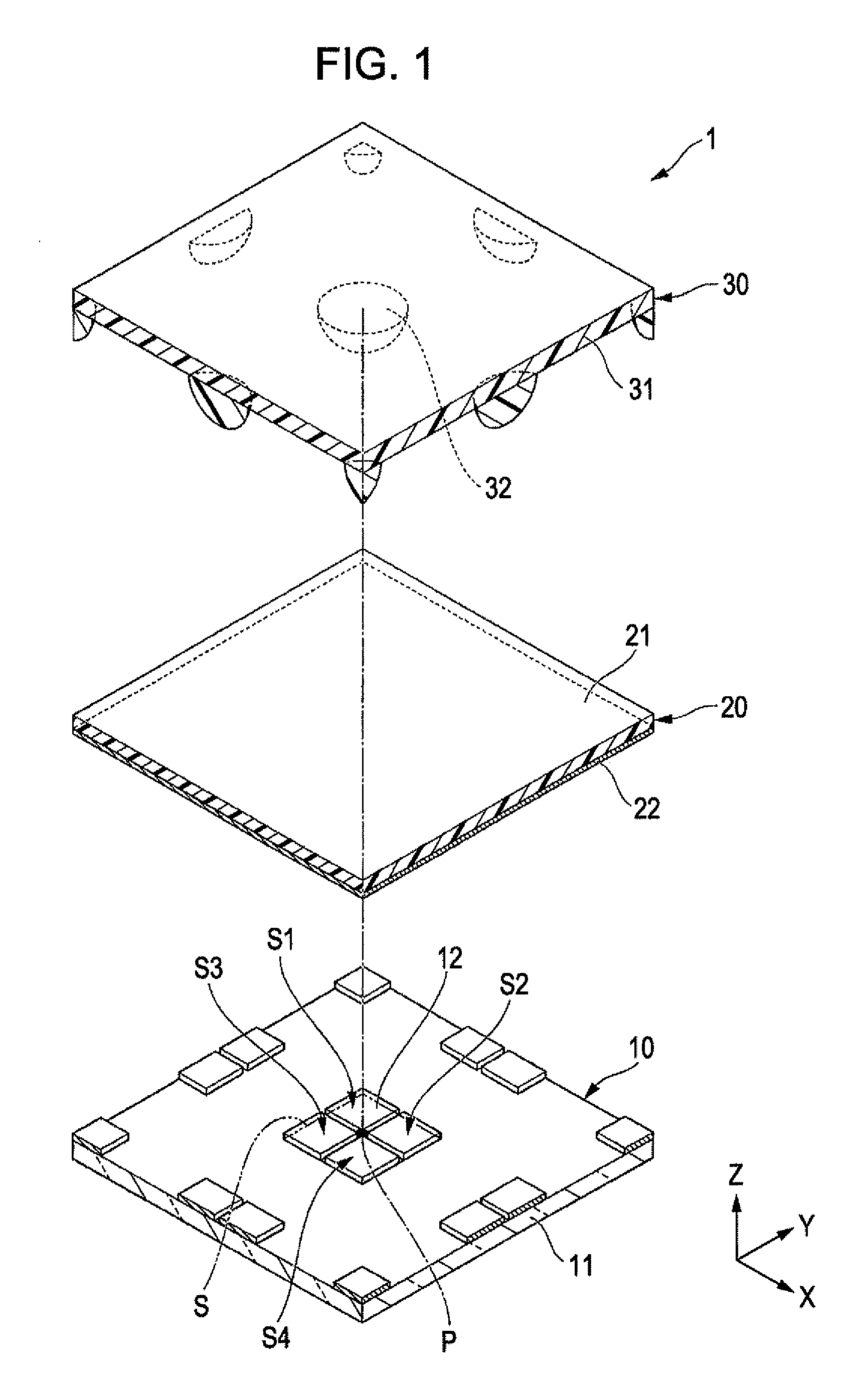
[0065]FIG. 1 is an exploded perspective view illustrating a schematic configuration of a detection device 1 according to a first embodiment of the invention. In FIG. 1, illustration of a dielectric body 40 is omitted for the purpose of simplicity (refer to FIG. 7). In FIG. 1, the reference symbol P denotes a reference point, and the reference symbol S denotes a unit detection area detected by a plurality of capacitance detection elements S1 to S4 (including a first capacitor electrode 12, a second capacitor electrode 22, and a dielectric body 40) arranged to match with a single elastic projection 32.
[0066]The detection device 1 is an electrostatic capacitance type touch pad for detecting a direction of the external pressure applied to the reference point, and is used as, for example, a pointing device instead of a mouse in electronic devices such as a laptop computer. In addition, the “reference point” refers to a point where a gravity center of the elastic projection is positioned ...
second embodiment
[0122]FIG. 12 is an exploded perspective view illustrating a schematic configuration of the detection device 2 according to a second embodiment of the invention in conjunction with FIG. 1. In FIG. 12, illustration of the dielectric body 40 (refer to FIG. 13) is omitted for the simplicity purpose. In FIG. 12, the reference symbol P denotes a reference point, and the reference symbol S denotes a unit detection area detected by a plurality of capacitance detection elements Si (including a first capacitor electrode 112, a second capacitor electrode 22, and a dielectric body 40) arranged to match with a single elastic projection 32. The detection device 2 according to the present embodiment is different from the detection device 1 described above in the first embodiment in that a plurality of first capacitor electrodes 112 are arranged in at least four rows and four columns along two perpendicular directions. In FIG. 12, like reference numerals denote like elements as in FIG. 1, and desc...
third embodiment
[0139]FIG. 16 is an exploded perspective view illustrating a schematic configuration of a detection device 3 according to a third embodiment of the invention in conjunction with FIG. 12. In FIG. 16, illustration of the dielectric body 40 (refer to FIGS. 17A to 17C) will be omitted for the simplicity purpose. In addition, in FIG. 16, the reference symbol P denotes a reference point, and the reference symbol S denotes a unit detection area detected by a plurality of capacitance detection elements Si (including a first capacitor electrode 112, a second capacitor electrode 22, and a dielectric body 40) arranged to match with a single elastic projection 32. The detection device 3 according to the present embodiment is different from the detection device 2 described above in the second embodiment in that a spacer 50 is arranged in at least a boundary with the adjacent elastic projection 32 between the first and second substrates 110 and 20. In FIG. 16, like reference numerals denote like ...
PUM
 Abstract
Description
Claims
Application Information


