Stack package and semiconductor package including the same

a technology of semiconductor and stack package, which is applied in the direction of semiconductor/solid-state device details, semiconductor devices, electrical apparatus, etc., and can solve problems such as serious damag

Active Publication Date: 2012-01-26
SAMSUNG ELECTRONICS CO LTD
View PDF3 Cites 165 Cited by
  • Summary
  • Abstract
  • Description
  • Claims
  • Application Information

AI Technical Summary

Benefits of technology

[0007]The inventive concept provides a stack package including a supporter to prevent warpage, the supporter being fixed onto a first semiconductor chip on which a second semiconductor chip is stacked.

Problems solved by technology

However, since the rigidity of silicon (Si) is weak, warpage may be seriously caused due to a difference in the coefficients of thermal expansion (CTE) of a semiconductor chip and a molding member.

Method used


Image

  • Stack package and semiconductor package including the same
  • Stack package and semiconductor package including the same
  • Stack package and semiconductor package including the same

Examples


Embodiment Construction

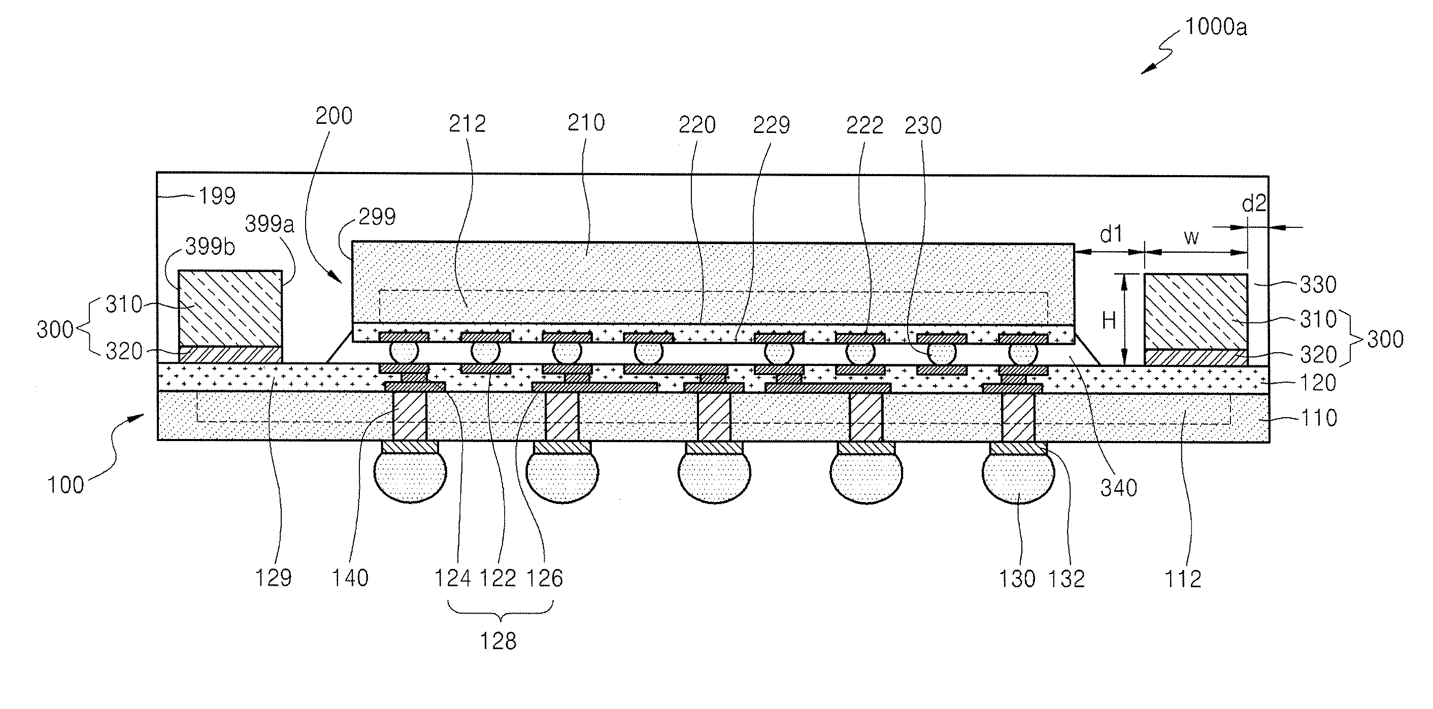
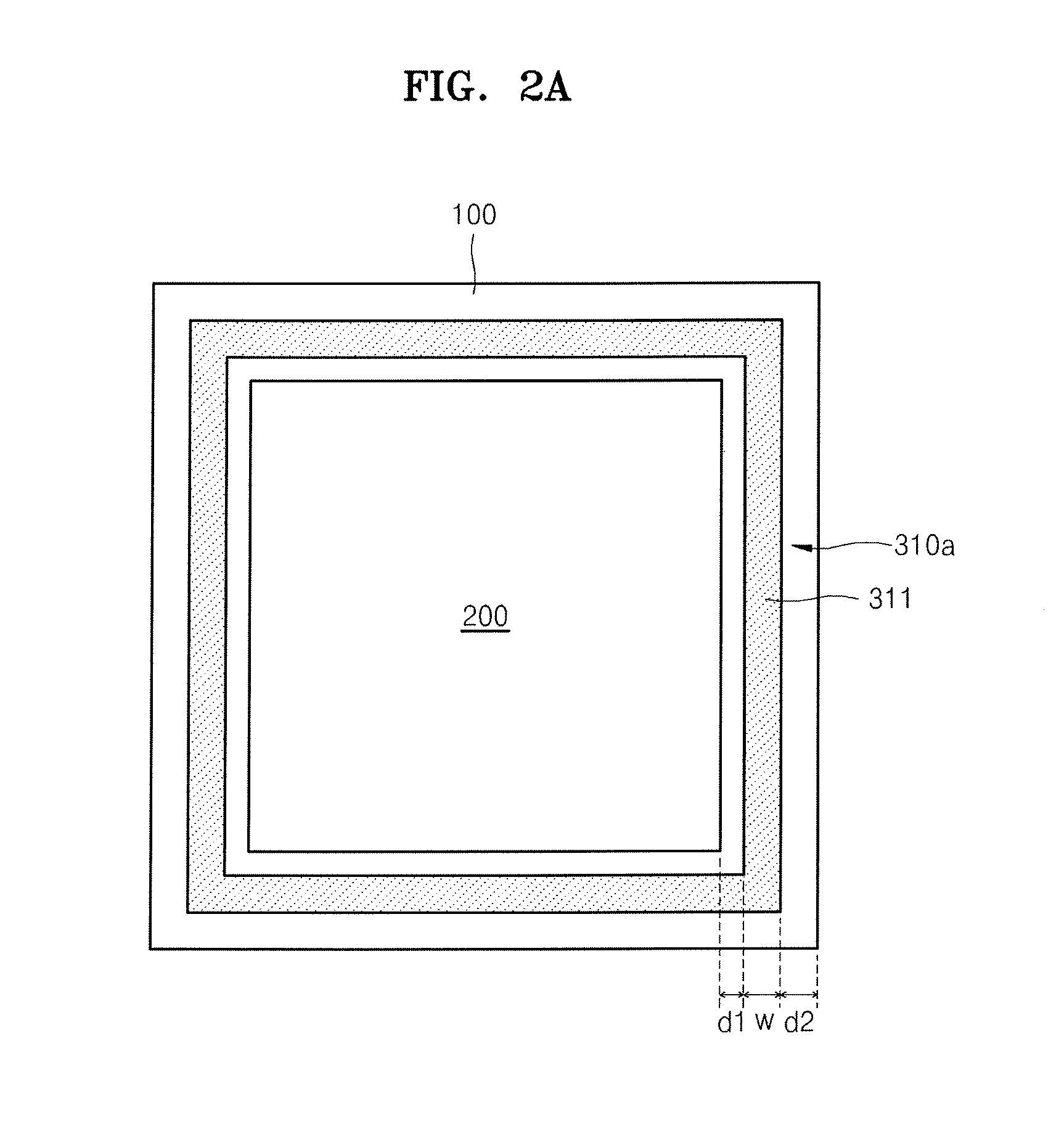
[0049]Hereinafter, a stack package, a semiconductor package, and a method of manufacturing the semiconductor package will be described with regard to exemplary embodiments of the inventive concept with reference to the attached drawings. It will be understood that various changes in form and details may be made, and thus, exemplary embodiments will be illustrated in diagrams, and will be described with reference to the diagrams.

[0050]Reference will now be made in detail to example embodiments, examples of which are illustrated in the accompanying drawings. However, the inventive concept is not limited to the embodiments described hereinafter, and the embodiments herein are rather introduced to provide easy and complete understanding of the scope and spirit of the inventive concept.

[0051]The terminology used herein is for the purpose of describing particular embodiments only and is not intended to be limiting of the inventive concept. As used herein, the singular forms “a,”“an” and “...


PUM


Abstract

A stack package usable in a three-dimensional (3D) system-in-package (SIP) includes a first semiconductor chip, a second semiconductor chip, and a supporter. The first semiconductor chip includes a through silicon via (TSV), and the second semiconductor chip is stacked on the first semiconductor chip and is electrically connected to the first semiconductor chip through the TSV of the first semiconductor chip. The supporter is attached onto the first semiconductor chip so as to be spaced apart from an edge of the second semiconductor chip.

Description

CROSS-REFERENCE TO RELATED APPLICATIONS[0001]This application claims priority under 35 U.S.C. §119 from Korean Patent Application No. 10-2010-0070471, filed on Jul. 21, 2010, in the Korean Intellectual Property Office, the disclosure of which is incorporated herein in its entirety by reference.BACKGROUND OF THE INVENTION[0002]1. Field of the Invention[0003]The inventive concept relates to a stack package, and a semiconductor package including the stack package, and more particularly, to a stack package including a supporter attached onto a first semiconductor chip on which a second semiconductor chip is stacked, and a semiconductor package including the stack package.[0004]2. Description of the Related Art[0005]Along with the developments of high-speed and highly-integrated semiconductor devices, methods to connect semiconductor chips in a semiconductor package have been developed. Such methods include a conventional wire bonding method, a package-on-package (PoP) method, and a syst...

Claims


Application Information

Patent Timeline
Patent Type & Authority Applications(United States)
IPC IPC(8): H01L23/58
CPCH01L25/0655H01L2924/00014H01L25/105H01L2224/0557H01L2224/48227H01L2224/73204H01L2224/73265H01L2224/97H01L2225/06565H01L2924/09701H01L2924/15311H01L2924/15331H01L25/0657H01L2224/0401H01L2924/18161H01L24/97H01L2225/1094H01L2225/107H01L2225/1023H01L2924/3511H01L2224/73253H01L2224/32245H01L2224/32225H01L2224/32145H01L2224/16225H01L2224/16145H01L2924/01087H01L2924/01019H01L2224/81H01L2924/00H01L2924/00012H01L2224/05552H01L21/561H01L23/16H01L23/3128H01L23/36H01L23/3675H01L23/4334H01L23/481H01L23/49816H01L23/49827H01L23/49833H01L23/562H01L24/73H01L2924/15787H01L2924/181H01L23/29
Inventor LEE, CHUNG-SUNKIM, JUNG-HWANIM, YUN-HYEOKHWANG, JI-HWANKIM, HYON-CHOLCHOI, KWANG-CHULCHOI, EUN-KYONGMIN, TAE-HONG
Owner SAMSUNG ELECTRONICS CO LTD
Why Eureka
Try Eureka