
Eureka
For R&D, Eureka makes reading and utilizing patents & technical documents easy.
Eureka AIR
Designed for self-driven R&D workflows. Generate viable solutions, solve complex R&D challenges, empower your innovation with AI.

Eureka Materials
Designed for material experts only. Revolutionize your material R&D, from search, analyze, to developing new materials.

TechResearch
Generate reliable direction feasibility study reports for your R&D in just a few steps.

TechSeek
Discover and master advanced knowledge NOW. Basics, ideas, possibilities, all at once.

TechMind
As an expert in R&D Theories, TechMind can generates customized viable solutions instantly.

TechRisk
Analyze your overall solution with one click, know your potential R&D risks in advance.

TechMonitor
Get weekly tech updates, stay abreast of the latest tech innovations and key insights.
Method for manufacturing light emitting diode
- Summary
- Abstract
- Description
- Claims
- Application Information
AI Technical Summary
Problems solved by technology
Method used
Image

Examples
Embodiment Construction
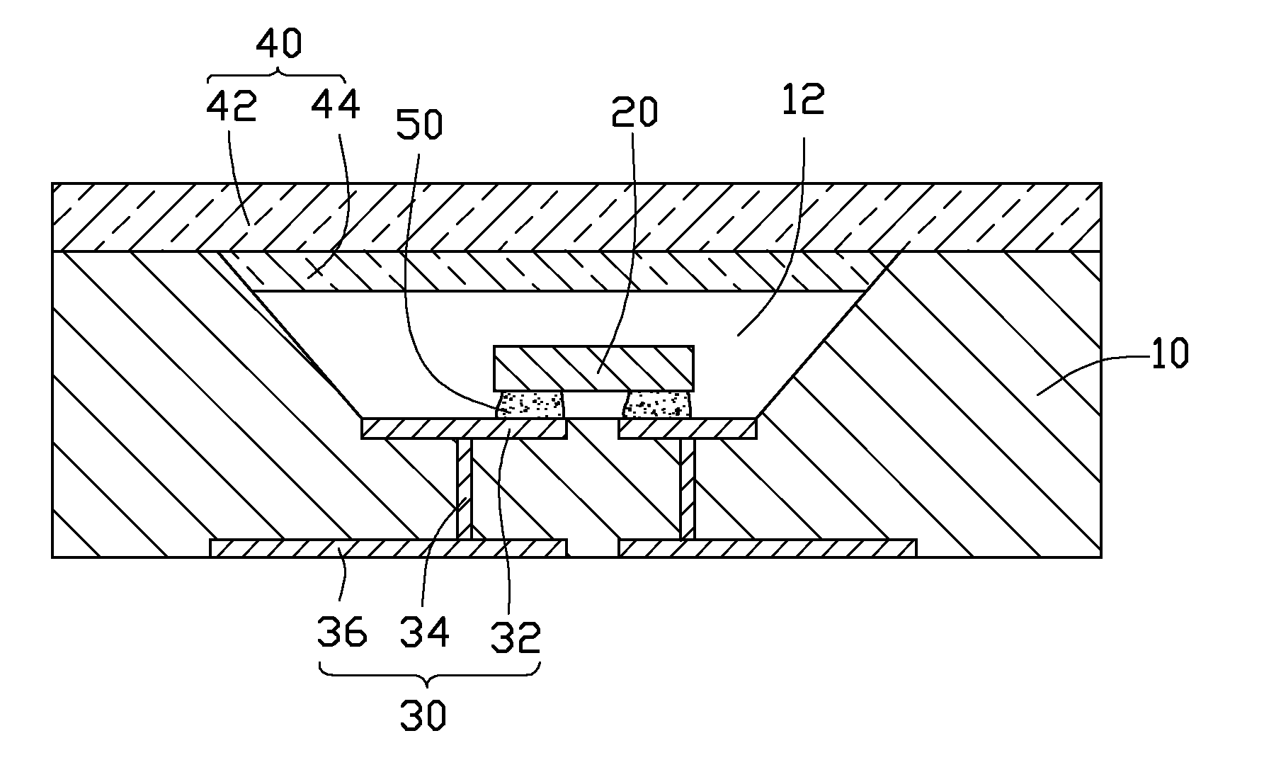
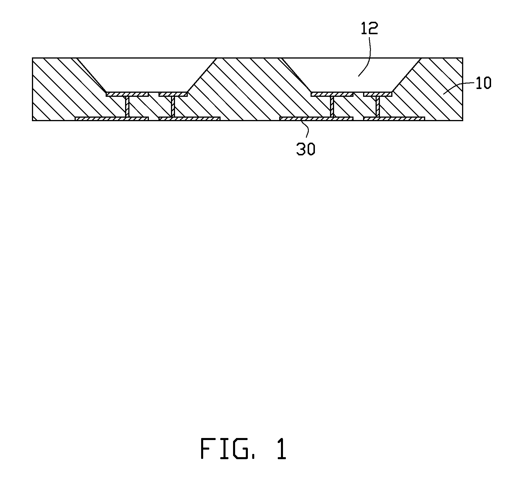
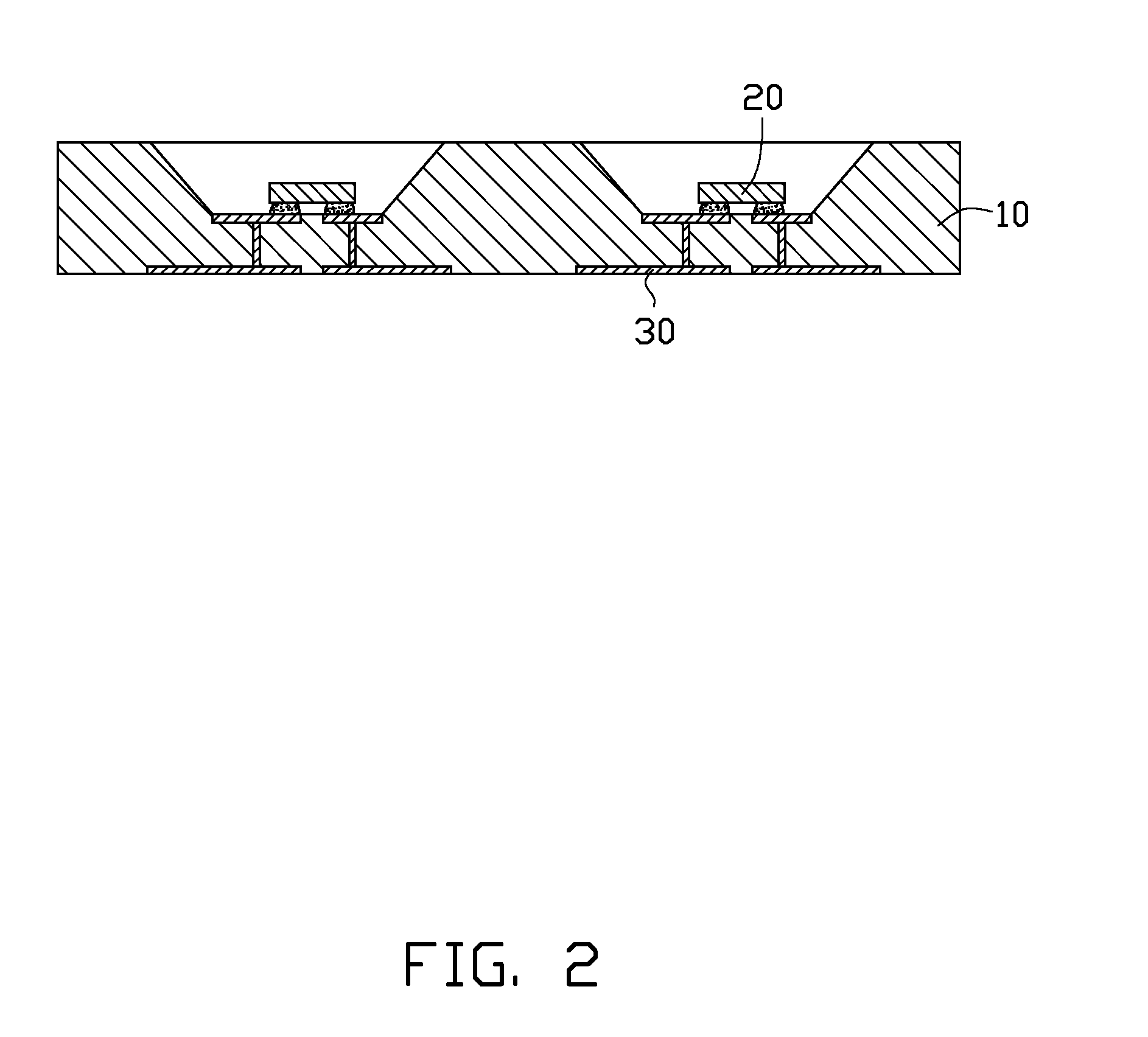
[0017]Referring to FIGS. 1-6, steps of a process for manufacturing an LED (light emitting diode) in accordance with a first embodiment of the present disclosure are disclosed.
[0018]Firstly, a base 10 having a plurality of pairs of leads 30 is provided as shown in FIG. 1. The base 10 may be made of Si or ceramic such as Al2O3 or AlN. The base 10 has a plurality of grooves 12 defined in a top face thereof. Each groove 12 has an inner diameter gradually increasing from a bottom towards a top of the base 10. Each pair of leads 30 are formed within the base 10 corresponding to each groove 12. Each lead 30 is made of electrically conductive materials such as copper, silver or gold. Each lead 30 includes a first conductive portion 32, a second conductive portion 36 parallel to the first conductive portion 32 and a connecting portion 34 connecting the first conductive portion 32 with the second conductive portion 36 (see FIG. 6). The first conductive portion 32 of the lead 30 is located at ...
PUM
 Abstract
Description
Claims
Application Information
 - R&D Engineer
- R&D Manager
- IP Professional
- Industry Leading Data Capabilities
- Powerful AI technology
- Patent DNA Extraction
Browse by: Latest US Patents, China's latest patents, Technical Efficacy Thesaurus, Application Domain, Technology Topic, Popular Technical Reports.
© 2024 PatSnap. All rights reserved.Legal|Privacy policy|Modern Slavery Act Transparency Statement|Sitemap|About US| Contact US: help@patsnap.com