Support body for semiconductor element, method for manufacturing the same and semiconductor device

Active Publication Date: 2005-05-05
NICHIA CORP
View PDF9 Cites 152 Cited by
  • Summary
  • Abstract
  • Description
  • Claims
  • Application Information

AI Technical Summary

Benefits of technology

[0032] The present invention provides a support body on which a semiconductor element can be mounted, that is made by separating a ceramics substrate whereon conductors are disposed, wherein a side face of the support body has a incised portion located on the side where the semiconductor element is to be mounted, and a portion cleaved substantially at right angles to the incised portion by applying a bending moment and a tensile force substantially simultaneously to the ceramics substrate, while the incised portion is in a range from ¼ to ¾ thickness of the ceramics substrate. With this constitution, the surface whereon the semiconductor element is to be mounted has uniform size because it is separated by the grooves. Also because the bending moment and the tensile force are applied substantially simultaneously, the support body can be made relatively easily without causing burrs or chippings in the cleavage surface. Keeping the incised portion small enables it to hold while the support body is allowed to have a large surface area on the side where the semiconductor element is mounted. In case a light emitting element is used for the semiconductor element, the light emitting device constituted by using the support body made of ceramics enables it to make an optical apparatus by mounting the semiconductor device on a circuit board without causing variability in the optical characteristics.
[0033] In the portion cleaved at right angles, it is preferable that a protruded portion protruding out from a vertical face extending vertically from the incised portion toward the opposite side to the side to be mounted with the semiconductor element are half of the thickness of the ceramics substrate or smaller in the portion cleaved at right angles. In a sideways emission type light emitting device in which the support body is used, if the protruded portion are half of the thickness of the ceramics substrate or smaller, a tilt on mounting is 30 degree or less. It is preferable that the protruded portion protruding out side are quarter of the thickness of the ceramics substrate or smaller. With this, the tilt on mounting is 15 degree or less. It is more preferable that the protruded portion pr

Problems solved by technology

This results in problems including the following major ones: (1) burrs and/or chippings are caused when cleaving the stack into individual support bodies; (2) cleavage surfaces cannot be made invariably smooth because burrs and chippings generated in the cleavage surface differ from chip to chip; and (3) the angle between the cleavage surface and the light emitting surface differ from chip to chip.
The cleavage surface having such problems as described above causes variability in the optical characteristics of the device when the light emitting device is mounted on a circuit board to make an optical device.
However, there occur such problems as a part of the light e

Method used


Image

  • Support body for semiconductor element, method for manufacturing the same and semiconductor device
  • Support body for semiconductor element, method for manufacturing the same and semiconductor device
  • Support body for semiconductor element, method for manufacturing the same and semiconductor device

Examples


example 1

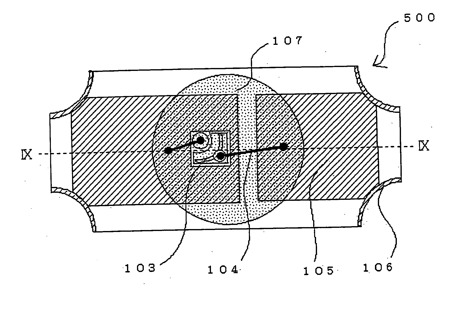
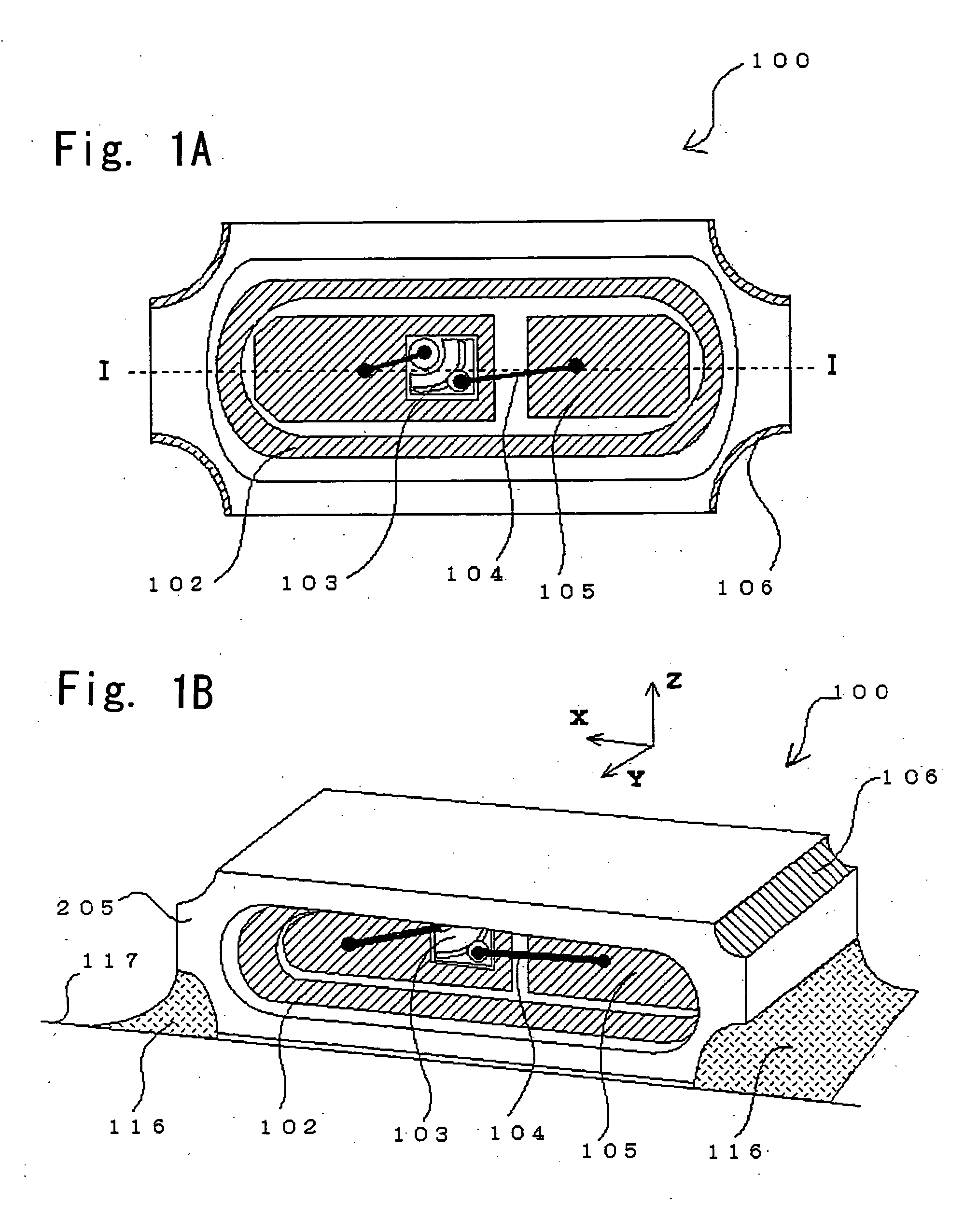
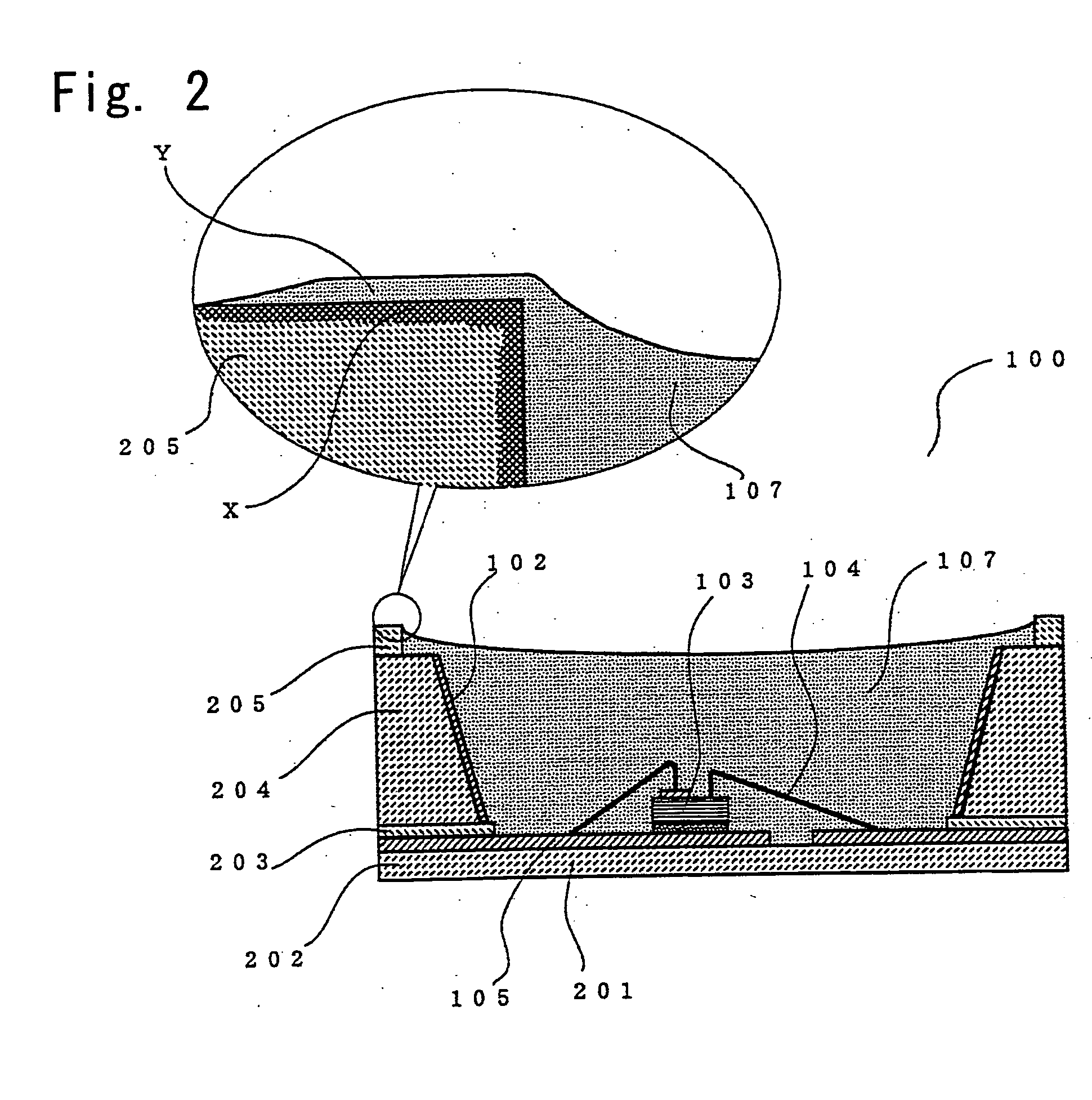
[0171] Example 1 of the present invention will be described with reference to the accompanying drawings. FIG. 1A is a schematic top view of a light emitting device 100 that uses the ceramics package and the light emitting element according to this embodiment. FIG. 2 is shows a sectional view taken along lines C-C′ in FIG. 1 and an enlarged sectional view of a portion around the top face of the recess side wall. FIG. 1B is a perspective view schematically showing the semiconductor device of this embodiment being electrically and mechanically connected by soldering to the mounting surface where the wiring pattern has been formed.

[0172] The ceramics package of this embodiment comprises at least a ceramics base 202 serving as the substrate, and a ceramics base 204 having through hole that widens toward the opening. The ceramics base 202 that serves as the substrate has the electrical wiring 105 for supplying power to the LED chip 103 running from the bottom of the recess on the package...

example 2

[0186]FIG. 8 is a schematic sectional view of the light emitting device of this example. The sealing member 107 of this example is formed so as to cover at least the light emitting element 103 without covering the reflecting surface 102. As indicated by Y in the enlarged sectional view of FIG. 8, the silicone resin covers the top face of the recess side wall of the ceramics package. In addition, a part of the silicone resin impregnates the ceramics base 204 that forms the top face of the recess side wall and forms an impregnated portion X. In this example, since the solder is restricted from creeping up by the silicone resin that covers the top face of the recess side wall, the solder that has been reflowed never touches the reflecting surface 102. Therefore, mounting can be carried out with high reliability as short-circuiting does not occur between positive and negative electrodes when mounting the device on an external circuit board that has electrical circuit formed thereon.

example 3

[0187] The light emitting device of this example is formed similarly to Examples 1 and 2, except for containing fluorescent material in the sealing member.

[0188] Stock material for the fluorescent material is made by coprecipitating a solution of a mixture of rare earth elements Y, Gd, Ce in stoichiometrical proportions dissolved in an acid with oxalic acid, firing the product of coprecipitation to obtained a coprecipitated oxide, and mixing it with aluminum oxide. This mixture, with a fluoride such as ammonium fluoride added thereto as a flux, is put into a crucible and fired at a temperature of about 1400° C. in air for three hours. The fired mixture is crushed in a ball mill in wet process, and undergoes the processes of washing, separation, drying and sieving, thereby to obtain a fluorescent material (Y0.995Gd0.005)2.750A15O12:Ce0.250 having median particle size of 8 μm.

[0189] 5.5% by weight of the fluorescent material (refractive index 1.84) is added to the silicone resin com...


PUM


Abstract

A semiconductor device comprising the semiconductor element and the support body made of a stack of ceramics layers having a recess in which a electrical conductors are electrically connected with the semiconductor element, wherein at least a part of the top face of the recess side wall is covered by a resin, thereby providing a light emitting device of high reliability.

Description

BACKGROUND OF THE INVENTION [0001] 1. Field of the Invention [0002] The present invention relates to a method of manufacturing a support body made of ceramics whereon a semiconductor element, particularly a semiconductor light emitting element can be mounted, and to a semiconductor device that employs the support body made of ceramics. [0003] 2. Description of the Related Art [0004] A support body made of ceramics for mounting a semiconductor element has been manufactured by stacking ceramics layers that have not yet been fired, called the ceramics green sheets, forming through holes in the stack, making electrical wiring to connect the semiconductor element and firing the stack. At the time when the ceramics green sheets have been stacked, cleaving lines are drawn so the stack of ceramic green sheets that has been fired can be cleaved by applying a force in a particular direction and separated into individual ceramics packages (refer, for example, to Patent Document 1). [0005] The ...

Claims


Application Information

Patent Timeline
IPC IPC(8): H01L21/48H01L23/02H01L23/04H01L23/08H01L23/498H01L33/32H01L33/50H01L33/56H01L33/60H05K3/34
CPCH01L23/49805H01L2924/07802H01L33/62H01L2224/48091H01L2224/48465H01L2224/49107H01L2224/73265H01L2924/01004H01L2924/01012H01L2924/0102H01L2924/01025H01L2924/01046H01L2924/01057H01L2924/01063H01L2924/01078H01L2924/01079H01L2924/19041H05K3/3442H05K2201/09181H05K2201/09954H05K2201/10106H01L33/486H01L2224/45169H01L2224/45147H01L2224/45124H01L24/45H01L2924/12041H05K3/284H01L2224/45144H01L2924/01068H01L2924/01067H01L2924/01066H01L2924/01021H01L2924/01019H01L2924/00014H01L2924/00H01L2224/45015H01L2924/12035H01L2924/12042H01L2924/12036H01L2924/181Y02P70/50H01L2924/00012
Inventor SAKANO, KENSHO
Owner NICHIA CORP
Why Eureka
Try Eureka