Packaging substrate having embedded passive component and fabrication method thereof

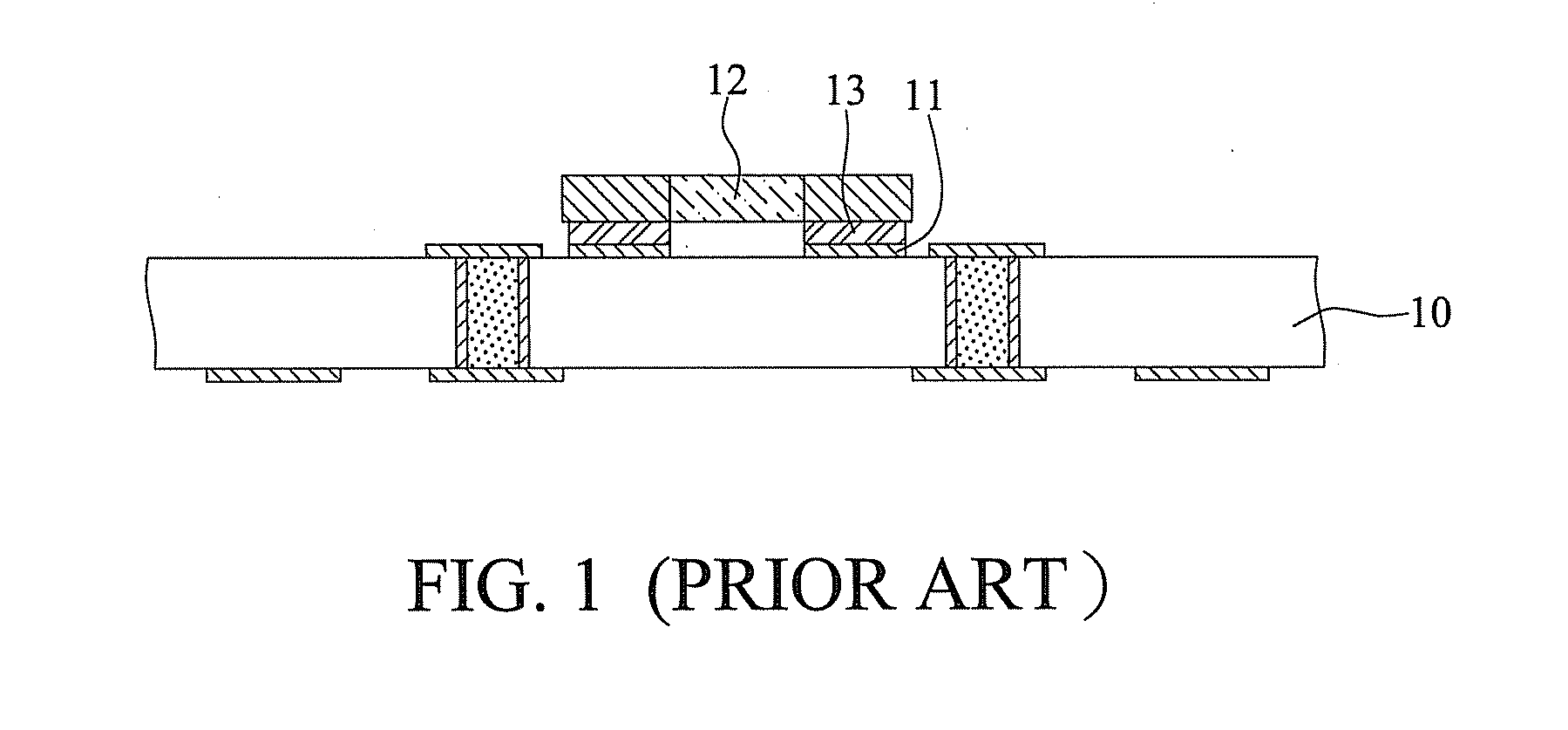
a technology of passive components and packaging substrates, which is applied in the manufacture of final products, printed electric components, and semiconductor/solid-state device details, etc., can solve the problems of increasing the height of the overall packaging structure, not meeting the minimization trend of electronic products, and adversely affecting the electrical performance of the structure, so as to shorten the signal transmission path and reduce the height

Active Publication Date: 2012-02-16
UNIMICRON TECH CORP
View PDF9 Cites 25 Cited by
  • Summary
  • Abstract
  • Description
  • Claims
  • Application Information

AI Technical Summary

Benefits of technology

[0027]Therefore, by embedding a passive component in a core board and a dielectric layer unit, the present invention provides a packaging substrate with reduced height, shortens the signal transmission path between the passive component and an inner wiring layer and accordingly allows more passive components to be disposed in such a packaging substrate without affecting the wiring layout.

Problems solved by technology

However, the passive component 12 mounted on the substrate 10 increases the height of the overall packaging structure, which does not meet the minimization trend of electronic products.
Further, since the passive component 12 is mounted on an outer surface of the substrate 10, it leads to a long signal transmission path between an inner circuit of the substrate 10 and the passive component, thereby adversely affecting the electrical performance of the structure.
In addition, the substrate 10 has conductive traces disposed on the surface thereof, thereby limiting the area available for mounting of the passive component 12.

Method used


Image

  • Packaging substrate having embedded passive component and fabrication method thereof
  • Packaging substrate having embedded passive component and fabrication method thereof
  • Packaging substrate having embedded passive component and fabrication method thereof

Examples


first embodiment

[0034]FIGS. 2A to 2G are cross-sectional views showing a fabrication method of a packaging substrate having at least an embedded passive component according to a first embodiment of the present invention.

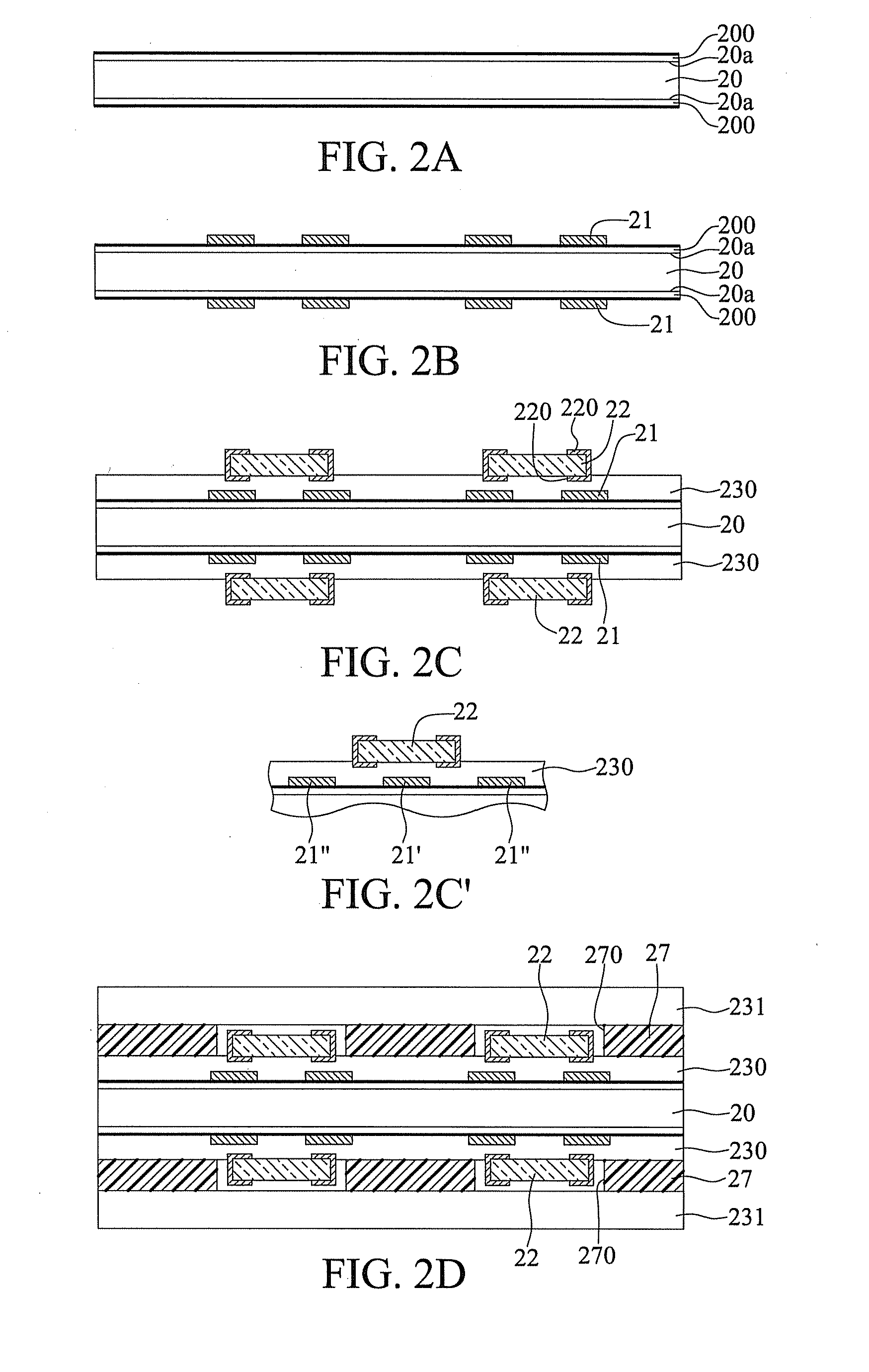
[0035]Referring to FIG. 2A, a carrier board 20 with two opposite surfaces 20a is provided, and a releasing film 200 and a metal layer 201 are sequentially formed on each of the two opposite surfaces 20a of the carrier board 20.

[0036]Referring to FIG. 2B, a plurality of positioning pads 21 is formed on each of the metal layers 201.

[0037]Referring to FIG. 2C, a first hot-melt dielectric layer 230 is formed to cover each of the metal layers 201 on the two opposite surfaces 20a of the carrier board 20; and at least a passive component 22 is disposed on each of the first hot-melt dielectric layers 230 at a position corresponding to the positioning pads 21, wherein the passive component 22 has upper and lower surfaces each having a plurality of electrode pads 220 disposed thereon, and the...

second embodiment

[0045]FIGS. 3A to 3G show a fabrication method of a packaging substrate having at least an embedded passive component according to a second embodiment of the present invention. In the present embodiment, solder bumps are formed instead of the positioning pads as in the first embodiment.

[0046]Referring to FIG. 3A, a carrier board 20 as shown in FIG. 2A is provided and a plurality of solder bumps 31 are formed on each of the metal layers 201 of the carrier board 20.

[0047]Referring to FIG. 3B, at least a passive component 22 as shown in FIG. 2C is disposed on the solder bumps 31 on each of the metal layers 201 via the electrode pads 220 of the lower surface thereof.

[0048]Referring to FIG. 3C, a first hot-melt dielectric layer 330 having at least an open area 330a is formed on each of the metal layers 201 such that the passive component 22 and the solder bumps 31 on the metal layer 201 are exposed from the open area 330a.

[0049]Referring to FIG. 3D, a core board 27 having at least a cav...

third embodiment

[0054]FIGS. 4A to 4D show a fabrication method of a packaging substrate having at least an embedded passive component according to a third embodiment of the present invention.

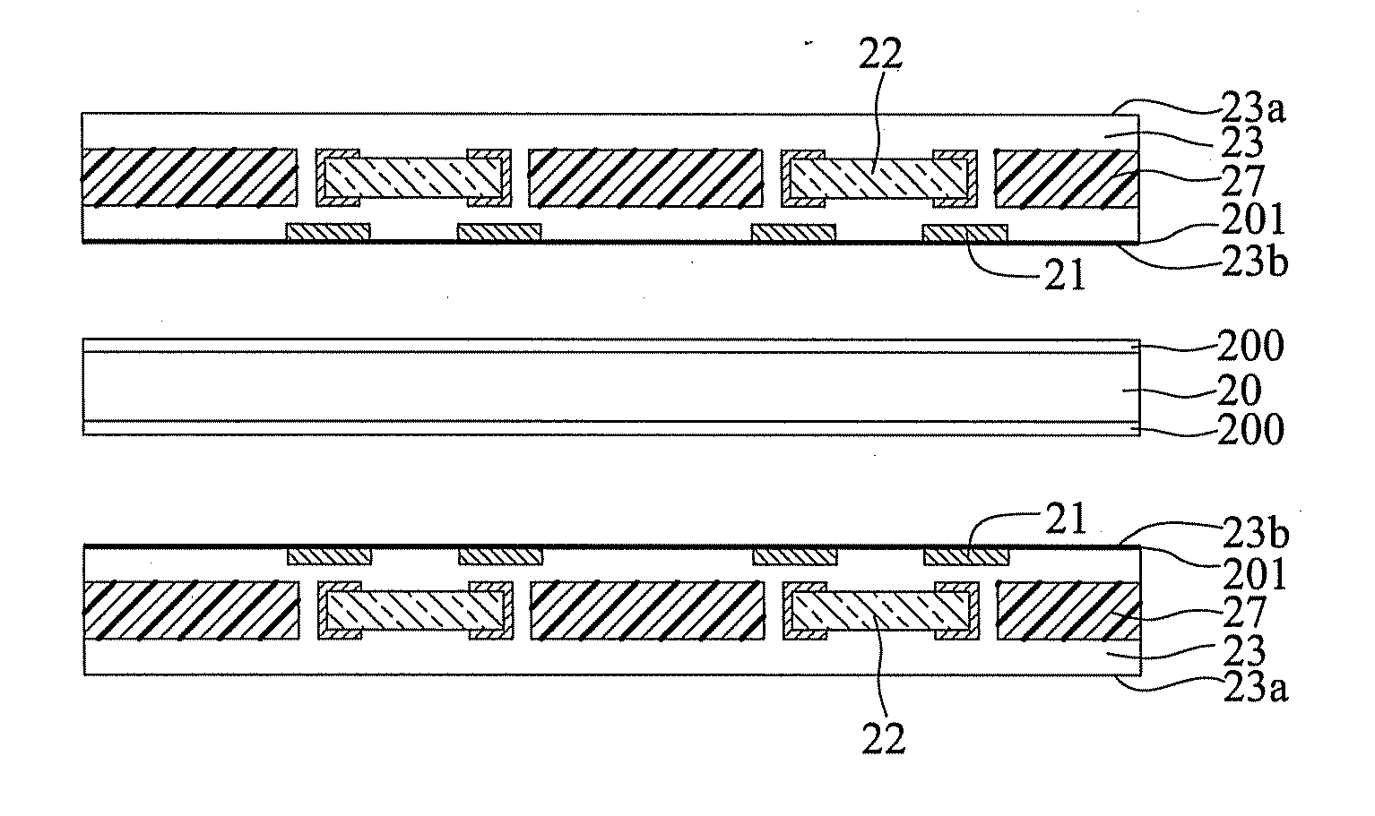
[0055]Referring to FIG. 4A, after the dielectric layer units 23 are formed by heat pressing as in FIG. 2D, a first wiring layer 44a is formed on the upper surface 23a of each of the dielectric layer units 23 and electrically connected to the electrode pads 220 of the upper surface of the passive component 22 through a plurality of first conductive vias 440a. Further, a built-up structure 45 is formed on each of the first wiring layers 44a, wherein the built-up structure 45 comprises at least a dielectric layer 450, a wiring layer 451 formed on the dielectric layer 450 and a plurality of conductive vias 452 disposed in the dielectric layer 450 for electrically connecting adjacent wiring layers.

[0056]Referring to FIG. 4B, the carrier board 20 and the releasing films 200 are removed so as to separate the two diele...


PUM

PropertyMeasurementUnit
conductiveaaaaaaaaaa
dielectricaaaaaaaaaa
hot-melt aaaaaaaaaa

Abstract

A packaging substrate includes: a core board with at least a cavity; a dielectric layer unit having upper and lower surfaces and encapsulating the core board and filling the cavity; a plurality of positioning pads embedded in the lower surface of the dielectric layer unit; at least a passive component having upper and lower surfaces with electrode pads disposed thereon and embedded in the dielectric layer unit so as to be received in the cavity of the core board at a position corresponding to the positioning pads; first and second wiring layers disposed on the upper and lower surfaces of the dielectric layer unit and electrically connected to the electrode pads of the upper and lower surfaces of the passive component through conductive vias, respectively. By embedding the passive component in the core board and the dielectric layer unit, the invention effectively reduces the height of the overall structure.

Description

BACKGROUND OF THE INVENTION[0001]1. Field of the Invention[0002]The present invention relates generally to packaging substrates and fabrication methods thereof, and more particularly, to a packaging substrate having at least an embedded passive component and a fabrication method thereof.[0003]2. Description of Related Art[0004]Passive components are increasingly demanded along with the development of semiconductor packaging technologies. Passive components, such as capacitors, resistors or inductors, allow signals to pass through without any change. In contrast to an active component, a passive component cannot control the flow of electrons. Therefore, when voltage or current changes, the resistance or impedance of the passive component does not change.[0005]Various products driven by electrical power require passive components for electronic loop control. The passive components can be applied in computer, communication and consumer electronic industries and so on. FIG. 1 shows a pa...

Claims


Application Information

Patent Timeline
Patent Type & Authority Applications(United States)
IPC IPC(8): H05K1/16H05K3/30
CPCH05K1/186Y02P70/611H05K2201/0195H05K2201/10015H05K2201/10636H01L23/49822H01L2924/00013H05K3/4682H05K3/32H05K3/4644Y10T29/4913H01L2924/0002H01L2224/13099H01L2224/13599H01L2224/05599H01L2224/05099H01L2224/29099H01L2224/29599H01L2924/00Y02P70/50
Inventor HSU, SHIH-PINGZENG, ZHAO-CHONG
Owner UNIMICRON TECH CORP
Why Eureka
Try Eureka