Transferring antenna structures to RFID components
What is AI technical title?
AI technical title is built by Patsnap AI team. It summarizes the technical point description of the patent document.
a technology of antenna structure and rfid, applied in the field of inlay substrates, can solve the problems of difficult volume production automation, high unreliability, and different geometrical dimensions of coils, and achieve the effect of facilitating the transfer of antenna structures
Inactive Publication Date: 2012-02-16
AMATECH GRP LTD
View PDF2 Cites 49 Cited by
Summary
Abstract
Description
Claims
Application Information
AI Technical Summary
This helps you quickly interpret patents by identifying the three key elements:
Problems solved by technology
Method used
Benefits of technology
Benefits of technology
[0050]In some embodiments of the invention, a method of forming RFID inlays may comprise: providing an inlay substrate comprising chip modules at transponder sites; providing an antenna substrate comprising antenna structures; transferring, such as by laminating or heating the structure of the antenna, antenna structures to the inlay substrate. After transferring the antenna structures, the antenna substrate may be removed. Termination ends of the antenna structures may be bonded to terminal areas of the chip module. The antenna substrate may be in sheet or web (reel) format. The antenna structures may comprise wire or other conductive material either on or in the antenna substrate. The antenna structures may be formed on the antenna substrate, or in a layer of adhesive on the antenna substrate. (Alternatively, the antenna structures may be formed such as by coil winding techniques, and disposed on the antenna substrate for sub...
Problems solved by technology
The coil winding process, may require pressing the coil into the substrate by means of heat and pressure, is highly unreliable, slow and difficult to automate for volume production.
The tooling is also subject to wear and tear resulting in coils having different geometrical dimensions.
One major disadvantage of the coil winding technique is the inability to form an antenna with a large pitch between the wire conductors which form the antenna.
Although common substrate techniques represent an improvement over coil winding in terms of antenna quality and throughput, a disadvantage is that different inlay formats require mechanical alterations to the production equipment resulting in downtime and inefficient use of the equipment, in particular where the number of transponder sites on a format is very low, as is the case in the production of inlays for electronic passports (“2up” or “3up” formats).
Also, embedding antenna wire in a substrate such as Teslin™ may be difficult.
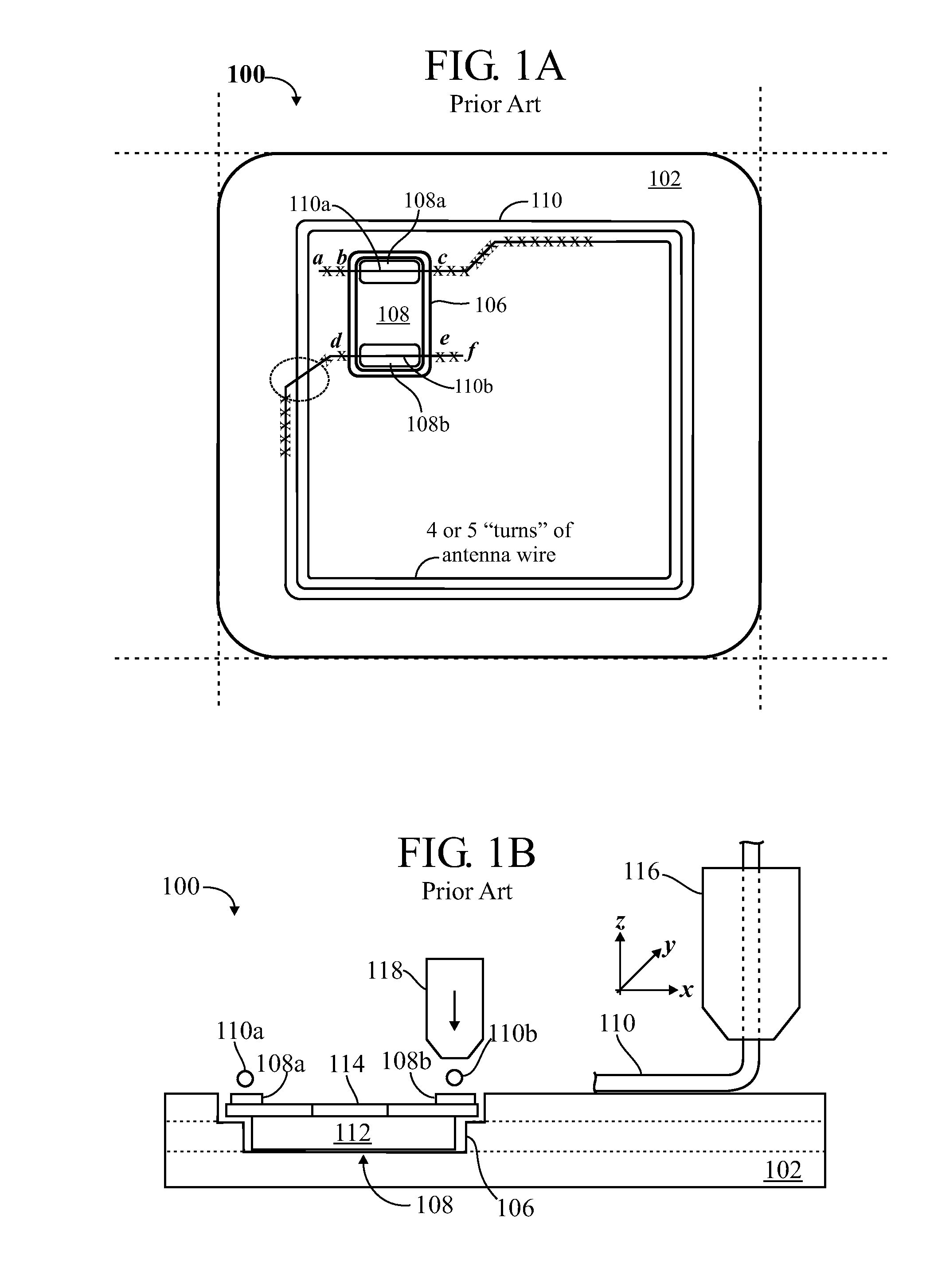
A difficulty with such a method is alignment of the wire ends with the terminal areas of a chip module, which may require manually aligning the wire ends for interconnection by hand.
Method used
Image
Click on the blue label to locate the original text in one second.
Reading with bidirectional positioning of images and text.
Examples
Embodiment Construction
[0094]Various embodiments will be described to illustrate teachings of the invention(s), and should be construed as illustrative rather than limiting. In the main, electronic passport covers with inlay substrates having leadframe modules may be used to illustrate the embodiments.
Forming Recesses in a Substrate
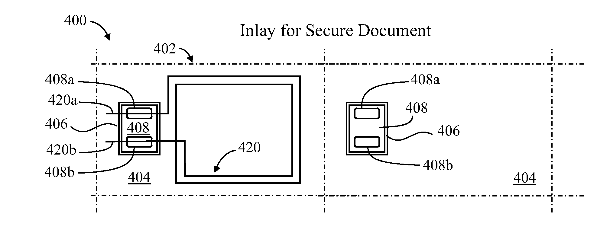
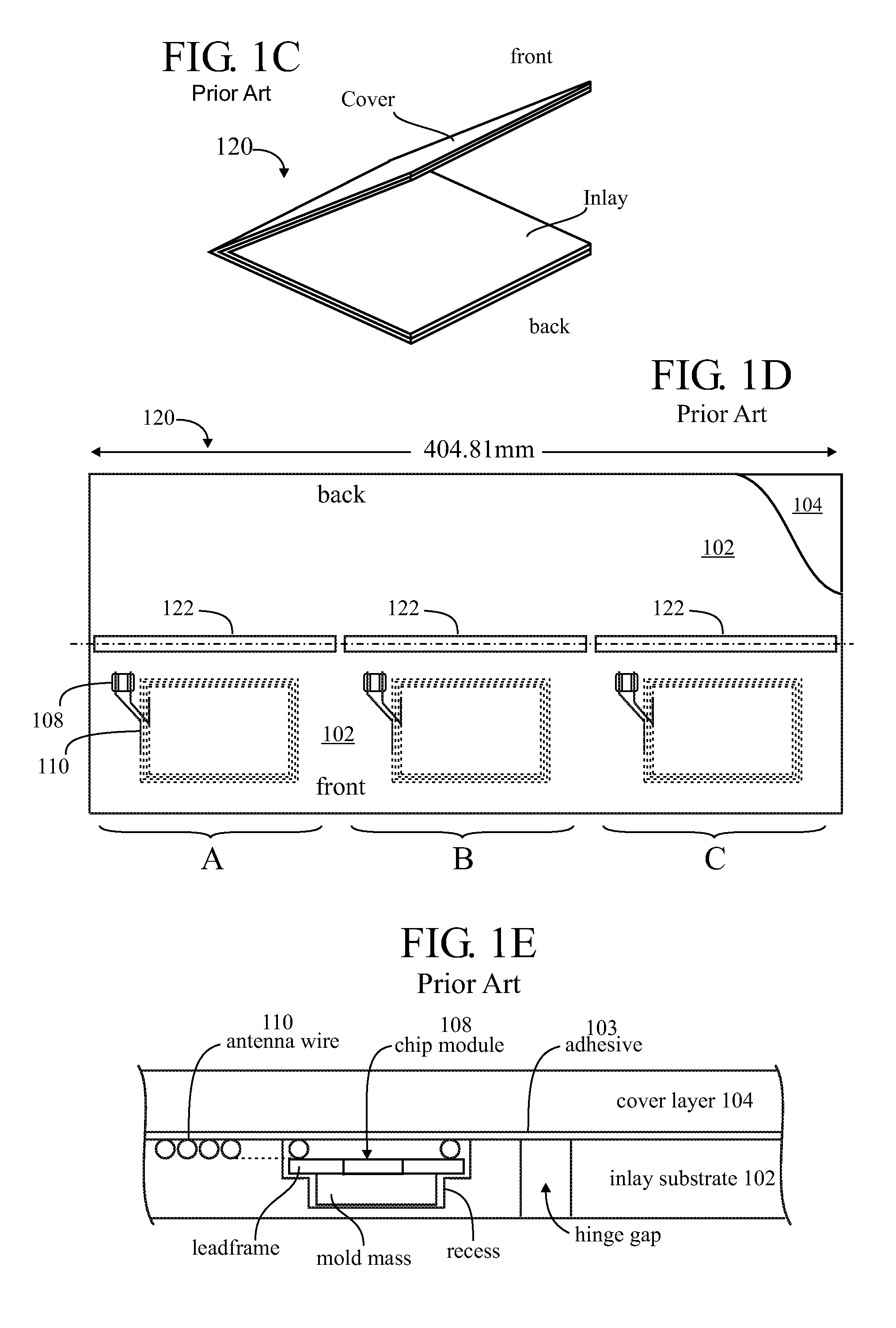
[0095]FIG. 2A illustrates a technique 200 for forming a recess 206 in a substrate 202 (such as an inlay substrate), using a laser 230. The inlay substrate 202 may be a single layer of Teslin™ (for example), having a thickness “t” of 356 μm. A typical size (width dimensions) for the recess 206, to accommodate a chip module with a lead frame, may be approximately 5 mm×8 mm The recess may extend completely through the inlay substrate, resulting in a “window-type” recess. The recess may extend only partially, such as 260 μm through the inlay substrate, resulting in a “pocket-type” recess (FIG. 1B illustrates a pocket-type recess).
[0096]The laser 230 emits a beam (dashed line), targ...
PUM
Property
Measurement
Unit
Thickness
aaaaa
aaaaa
Pressure
aaaaa
aaaaa
Size
aaaaa
aaaaa
Abstract
Forming antenna structures having turns of wire, foil or conductive material on a an antenna substrate or in a layer of adhesive layer on a carrier substrate, transferring the antenna structures individually or many at once to corresponding transponder sites on an inlay substrate and connecting the aligned termination ends of the antenna structures to terminal areas of RFID chip modules at the transponder sites. Transferring may be performed by various means such as laminating (heat and pressure), or heating the antenna structures directly or indirectly. The antenna substrate may be in web format or sheet format. Automated manufacturing procedures are disclosed. Kits having components for manufacturing inlay substrates, inlays and secure documents are disclosed. Various features of an inlay substrate and chip module are disclosed.
Application Information
Patent Timeline
Application Date:The date an application was filed.
Publication Date:The date a patent or application was officially published.
First Publication Date:The earliest publication date of a patent with the same application number.
Issue Date:Publication date of the patent grant document.
PCT Entry Date:The Entry date of PCT National Phase.
Estimated Expiry Date:The statutory expiry date of a patent right according to the Patent Law, and it is the longest term of protection that the patent right can achieve without the termination of the patent right due to other reasons(Term extension factor has been taken into account ).
Invalid Date:Actual expiry date is based on effective date or publication date of legal transaction data of invalid patent.

