Partially Depleted Dielectric Resurf LDMOS

a dielectric and dielectric technology, applied in the field of integrated circuit devices, can solve the problems of increasing on-resistance, difficult to integrate with low-voltage circuitry on the same chip,

Active Publication Date: 2012-02-23
NXP USA INC
View PDF5 Cites 79 Cited by
  • Summary
  • Abstract
  • Description
  • Claims
  • Application Information

AI Technical Summary

Problems solved by technology

But such LDMOS devices usually require thick and low-doped epitaxial layer, which makes them difficult to integrate with low-voltage circuitry on the same chip.
In addition, there are typically tradeoffs posed when integrating LDMOS devices between the on-resistance and breakdown voltage parameters of such devices, where the on-resistance is ideally kept lo

Method used


Image

  • Partially Depleted Dielectric Resurf LDMOS
  • Partially Depleted Dielectric Resurf LDMOS
  • Partially Depleted Dielectric Resurf LDMOS

Examples


Embodiment Construction

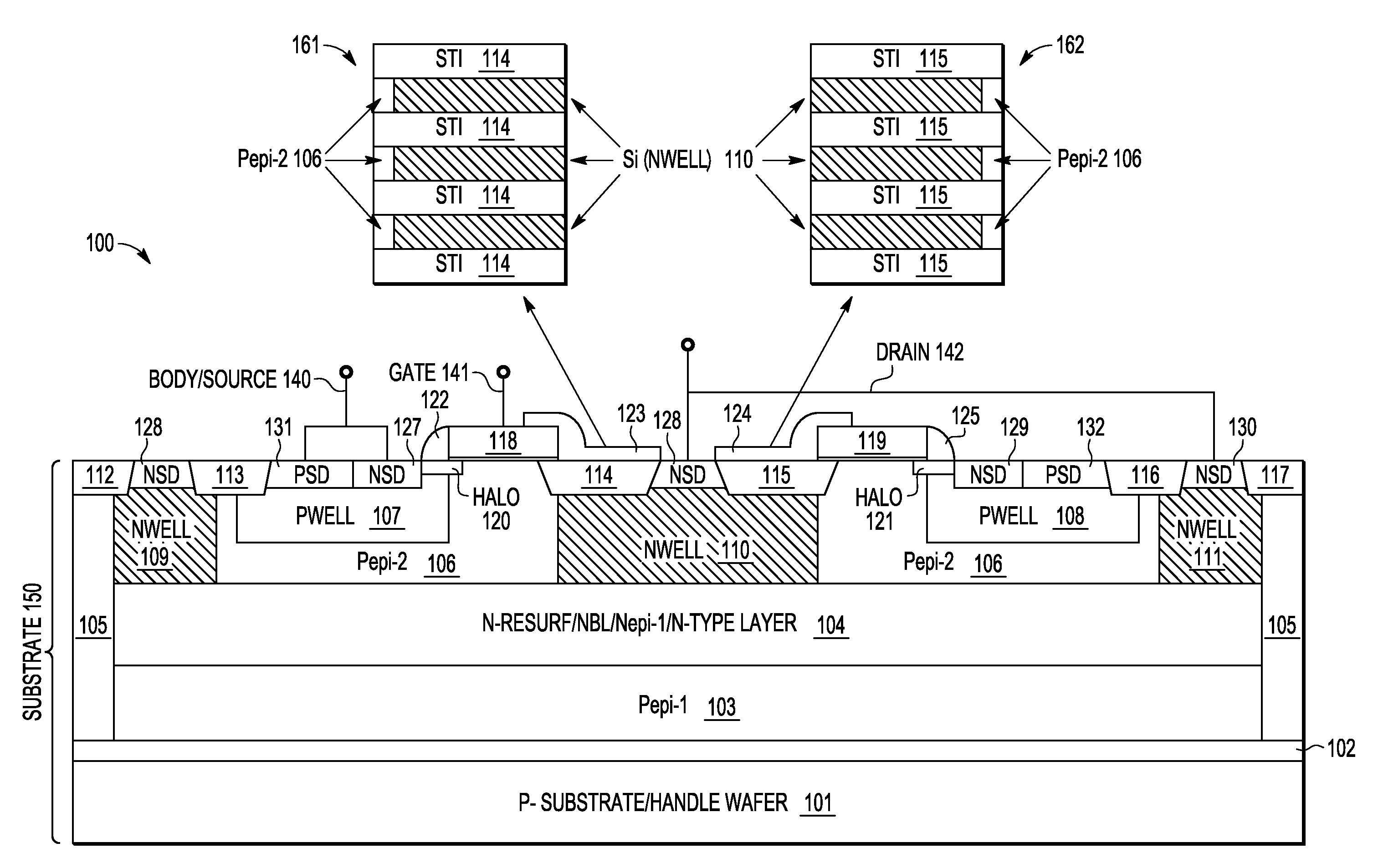
[0011]An N-Channel laterally diffused MOS (NLDMOS) transistor with a partially depleted dielectric RESURF (Dieler) drain extension structure is described for use with high voltage (e.g., approximately 15V or greater) smart power applications. The disclosed LDMOS transistor includes a dielectric RESURF drain extension structure having a plurality of STI stripes formed in a deeper low voltage n-well drain extension region. With the STI stripes positioned across the n-well and adjacent p-type region under the intended gate area to form narrow p-n diode strips, wider depletion widths and increased breakdown voltages are obtained. To further increase the breakdown voltage between the n-well and p-well regions, the p-well is pulled away from the n-well by disposing the p-well in a lightly doped p-type buffer region (e.g., p-epi buffer layer), thereby partially depleting the n-well drift region. By positioning the p-well within the p-type buffer region to be aligned with the source-side ga...


PUM


Abstract

An partially depleted Dieler LDMOSFET transistor (100) is provided which includes a substrate (150), a drift region (110) surrounding a drain region (128), a first well region (107) surrounding source region (127), a well buffer region (106) separating the drift region and first well region to at least partly define a first channel region, a gate electrode (118) formed over the first channel region having a source-side gate edge aligned with the first well region (107), an LDD extension region (120) extending from the source region to the channel region, and a dielectric RESURF drain extension structure (161) formed at the drain of the gate electrode (118) using the plurality of STI stripes (114).

Description

BACKGROUND OF THE INVENTION[0001]1. Field of the Invention[0002]The present invention is directed in general to integrated circuit devices and methods for manufacturing same. In one aspect, the present invention relates to the manufacture and use of laterally diffused MOS transistor (LDMOSFET) devices employing reduced surface field (RESURF) structures.[0003]2. Description of the Related Art[0004]High-voltage integrated circuits applications, such as high-voltage smart power applications, are constructed with integrated circuit MOS field effect transistor devices which must be able to sustain high voltages (e.g., fifty volts or greater) across the transistor device's source, body, gate, and drain terminals. With such high-voltage applications, laterally diffused MOS (LDMOS) transistor devices are often used to provide the high-voltage transistor devices. But such LDMOS devices usually require thick and low-doped epitaxial layer, which makes them difficult to integrate with low-volta...

Claims


Application Information

Patent Timeline
IPC IPC(8): H01L29/78H01L21/336
CPCH01L29/0653H01L29/0692H01L29/0847H01L29/1083H01L29/66659H01L2924/0002H01L29/7835H01L2924/00H01L29/0873
Inventor YANG, HONGNINGZUO, JIANG-KAI
Owner NXP USA INC
Why Eureka
Try Eureka