

Acoustic wave resonator and duplexer using same
- Summary
- Abstract
- Description
- Claims
- Application Information
AI Technical Summary
Benefits of technology
Problems solved by technology
Method used
Image

Examples
first exemplary embodiment
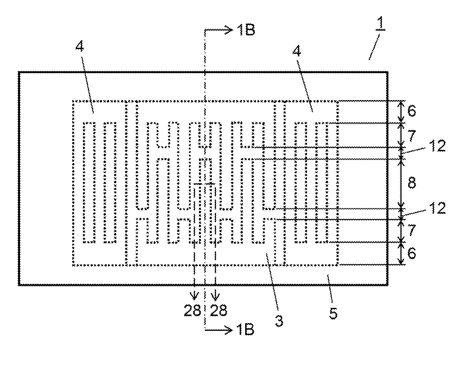
[0073]Hereinafter, a description is made of the first exemplary embodiment of the present invention using the related drawings. FIG. 1A is a top view of an acoustic wave resonator according to the first embodiment; FIG. 1B is a cross sectional (a cross section along the direction in which the electrode fingers of IDT electrode 3 extend) view of the acoustic wave resonator, taken along line 1B-1B in FIG. 1A.
[0074]In FIGS. 1A and 1B, acoustic wave resonator 1 includes piezoelectric body 2; IDT electrode 3 provided on piezoelectric body 2, for exciting an acoustic wave with wavelength λ; grating reflector 4 provided on piezoelectric body 2 so as to interpose IDT electrode 3; and dielectric thin film 5 provided on piezoelectric body 2 so as to cover IDT electrode 3 and grating reflector 4.
[0075]Piezoelectric body 2 is a substrate based on lithium niobate (LiNbO3); however, body 2 may be another piezoelectric single-crystal medium such as a substrate or thin film based on crystal, lithiu...
second exemplary embodiment
[0100]Next, a description is made of acoustic wave resonator 1 of the second exemplary embodiment using the related drawings. The configuration is the same as that of the first embodiment unless particularly described. FIG. 12A is a top view of acoustic wave resonator 1 according to the second embodiment; FIG. 12B is a cross sectional (a cross section along the direction in which the electrode fingers of IDT electrode 3 extend) view of the acoustic wave resonator, taken along line 12B-12B in FIG. 12A.
[0101]As shown in FIGS. 12A and 12B, acoustic wave resonator 1 of the second embodiment does not have a dummy electrode, and the entire region interposed between bus bar electrode region 6 and IDT cross region 8 becomes gap region 12. Here as well, normalized film thickness 10 of dielectric thin film 5 above a part of at least one (both in FIG. 12) of bus bar electrode region 6 and gap region 12 (the side of bus bar electrode region 6) is configured to be smaller than normalized film th...
third exemplary embodiment
[0104]Next, a description is made of acoustic wave resonator 1 of the third exemplary embodiment using the related drawings. The configuration is the same as that of the first embodiment unless particularly described. FIG. 13 is a cross sectional (a cross section of IDT cross region 8) view, taken along line 13-13 in FIG. 1A according to the first embodiment or line 13-13 in FIG. 12A according to the second embodiment.
[0105]In acoustic wave resonator 1 of FIG. 13, piezoelectric body 2 is based on lithium niobate (LiNbO3), and the Euler angle (φ, θ, ψ) of this piezoelectric body 2 satisfies −100°≦θ≦−60°, 1.193φ−2°≦ψ≦1.193φ+2°, ψ≦−2φ−3°, −2φ+3°≦ψ where φ and θ are cut-out angles of piezoelectric body 2; ψ is the propagation angle of a main acoustic wave in IDT electrode 3 on piezoelectric body 2.
[0106]Here, piezoelectric body 2 based on lithium niobate is a trigonal crystal, and thus the Euler angle has the next relationship.
(ϕ,θ,Ψ)=(60+ϕ,-θ,Ψ)=(60-ϕ,-θ,180-Ψ)=(ϕ,180+θ,180-Ψ)=(ϕ,θ,180...
PUM
 Abstract
Description
Claims
Application Information