Sensing Circuit For Programmable Resistive Device Using Diode as Program Selector

a technology of resistive device and sensing circuit, which is applied in semiconductor devices, digital storage, instruments, etc., can solve the problems of large cell size of electrical fuse using silicided polysilicon, high cost of embedded pcm applications, and complicated process steps of diodes, etc., to achieve the effect of reducing cell size and cos

Active Publication Date: 2012-02-23
ATTOPSEMI TECH CO LTD
View PDF4 Cites 80 Cited by
  • Summary
  • Abstract
  • Description
  • Claims
  • Application Information

AI Technical Summary

Benefits of technology

[0016]Embodiments of programmable resistive device cells using polysilicon diodes as program selectors are disclosed. The programmable resistive devices can be fabricated using standard CMOS logic processes to reduce cell size and cost.
[0017]In one embodiment, a programmable resistive device and memory can use diodes fabricated on a polysilicon as program selectors, where the P and N terminals of the diode are P+ and N+ implants on the same polysilicon. The same P+ and N+ implants are used to create sources or drains of core logic PMOS and NMOS devices, respectively. Advantageously, the same polysilicon can be used to create CMOS gates in standard CMOS logic processes. By using polysilicon diodes in standard CMOS processes, a small cell size can be achieved, without incurring any special processing or masks. Thus, costs can be reduced substantially for variously applications, such as embedded applications.

Problems solved by technology

As a result, the cell size of an electrical fuse using silicided polysilicon tends to be very large.
Though this technology can reduce the PCM cell size to only 6.8 F2 (F stands for feature size), the diode requires very complicated process steps, such as Selective Epitaxial Growth (SEG), to fabricate, which would be very costly for embedded PCM applications.
The fuse elements 80, 84 in FIGS. 3(a) and 3(b) are relatively large structures which makes them unsuitable for some applications.

Method used


Image

  • Sensing Circuit For Programmable Resistive Device Using Diode as Program Selector
  • Sensing Circuit For Programmable Resistive Device Using Diode as Program Selector
  • Sensing Circuit For Programmable Resistive Device Using Diode as Program Selector

Examples


Embodiment Construction

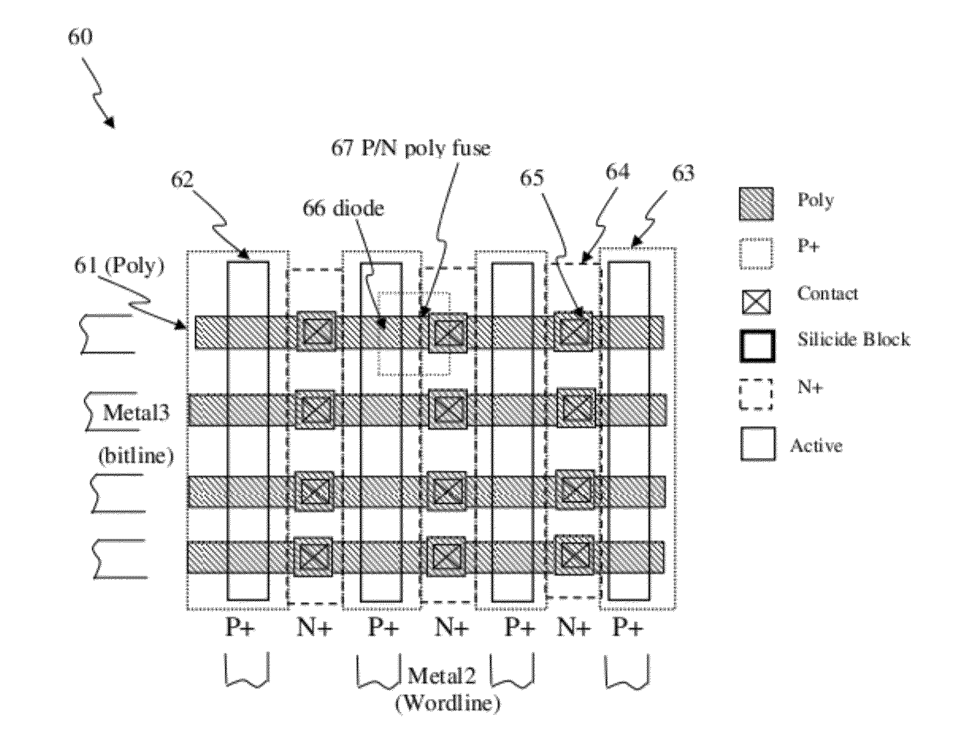
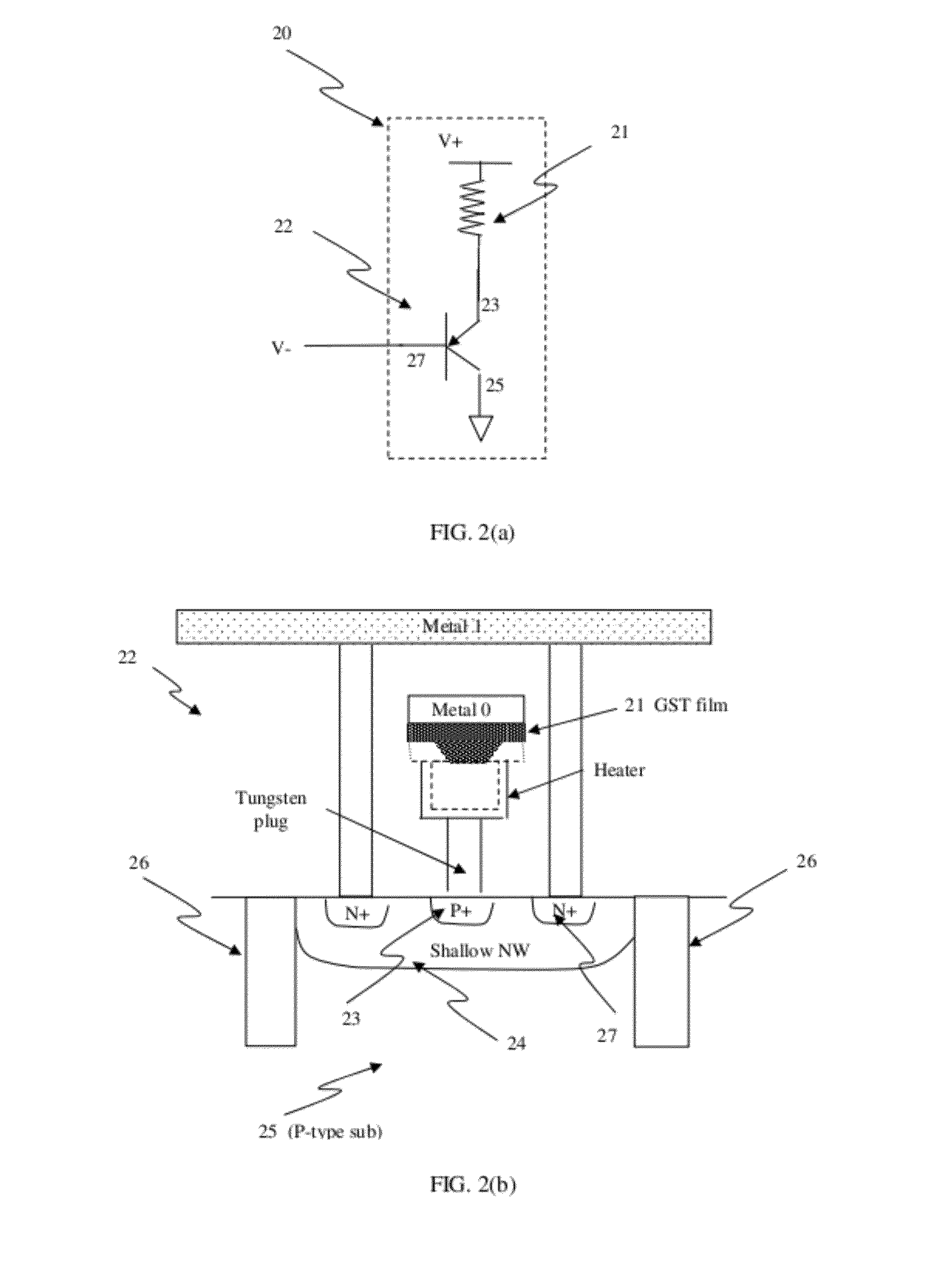
[0067]Embodiments disclosed herein use a polysilicon diode as program selector for a programmable resistive device. The diode can comprise P+ and N+ implants on a polysilicon substrate. Since the P+ and N+ implants and polysilicon are readily available in standard CMOS logic processes, these devices can be formed in an efficient and cost effective manner. There are no additional masks or process steps to save costs. The programmable resistive device can also be included within an electronic system.

[0068]According to one embodiment, a sensing circuit for programmable resistive device can use a diode as program selector. The sensing circuit can have a supply voltage VDDR of ˜2-3V, higher than ˜1.0V supply voltage for core logic devices. The sensing circuit can have a reference and a sensing branch. In one embodiment, each branch can have a first type of MOS with the source coupled to a first supply voltage, the drain coupled to the drain of a second type of MOS, which can have the gat...


PUM


Abstract

A sensing circuit for programmable resistive device using diode as program selector is disclosed. The sensing circuit can have a reference and a sensing branch. In one embodiment, each branch can have a first type of MOS with the source coupled to a first supply voltage, the drain coupled to the drain of a second type of MOS, which can have the gate coupled to a bias supply voltage. The sources of the second type of MOS in the reference and sensing branches can be coupled to a reference resistor and a programmable resistance element, respectively, and they are further coupled to a second supply voltage through their diodes. The gate of the first type of MOS in the sensing branch can be coupled to the gate of the first type of MOS in the reference branch, which can have the drain coupled to the gate. The resistance difference between the reference resistor and the programmable resistive element can be sensed through the drain of the first type of MOS in the sensing branch into a logic level.

Description

CROSS-REFERENCE TO RELATED APPLICATIONS[0001]This application claims priority benefit of U.S. Provisional Patent Application No. 61 / 375,653, filed on Aug. 20, 2010 and entitled “CIRCUIT AND SYSTEM OF USING JUNCTION DIODE AS PROGRAM SELECTOR FOR RESISTIVE DEVICES IN CMOS LOGIC PROCESSES,” which is hereby incorporated herein by reference; and U.S. Provisional Patent Application No. 61 / 375,660, filed on Aug. 20, 2010 and entitled “CIRCUIT AND SYSTEM OF USING POLYSILICON DIODE AS PROGRAM SELECTOR FOR RESISTIVE DEVICES IN CMOS LOGIC PROCESSES,” which is hereby incorporated herein by reference.BACKGROUND OF THE INVENTION[0002]1. Field of the Invention[0003]The present invention relates to programmable memory devices, such as programmable resistive devices for use in memory arrays.[0004]2. Description of the Related Art[0005]A programmable resistive device is generally referred to a device's resistance states that may change after means of programming. Resistance states can also be determi...

Claims


Application Information

Patent Timeline
Patent Type & Authority Applications(United States)
IPC IPC(8): G11C11/00
CPCG11C11/1659H01L27/2409G11C13/0004G11C13/0007G11C13/0011G11C13/0028G11C13/003G11C13/004G11C13/0069H01L29/785G11C11/1675G11C2013/0073G11C2213/72G11C2213/74G11C17/165G11C17/16H01L27/2436H01L45/06H01L45/144H01L45/04H01L45/085H01L45/1233H01L45/146H01L27/224G11C13/0002G11C8/14H10B61/10H10B63/20H10N70/231H10N70/826H10N70/8828H10B63/30H10N70/20H10N70/245H10N70/8833
Inventor CHUNG, SHINE C.
Owner ATTOPSEMI TECH CO LTD
Why Eureka
Try Eureka