Anti-tamper microchip package based on thermal nanofluids or fluids

Inactive Publication Date: 2012-03-22
I3 ELECTRONICS
View PDF10 Cites 24 Cited by
  • Summary
  • Abstract
  • Description
  • Claims
  • Application Information

AI Technical Summary

Benefits of technology

[0014]It is a primary object of the present invention to enhance the art of tamper-resistant electronic devices, which will be destroyed during a tampering event. A variety of fluids and nanofluids may be incorporated into the chip level package, such flu

Problems solved by technology

This fluid may attack and destroy components of the chip, such as silic

Method used


Image

  • Anti-tamper microchip package based on thermal nanofluids or fluids
  • Anti-tamper microchip package based on thermal nanofluids or fluids
  • Anti-tamper microchip package based on thermal nanofluids or fluids

Examples


Embodiment Construction

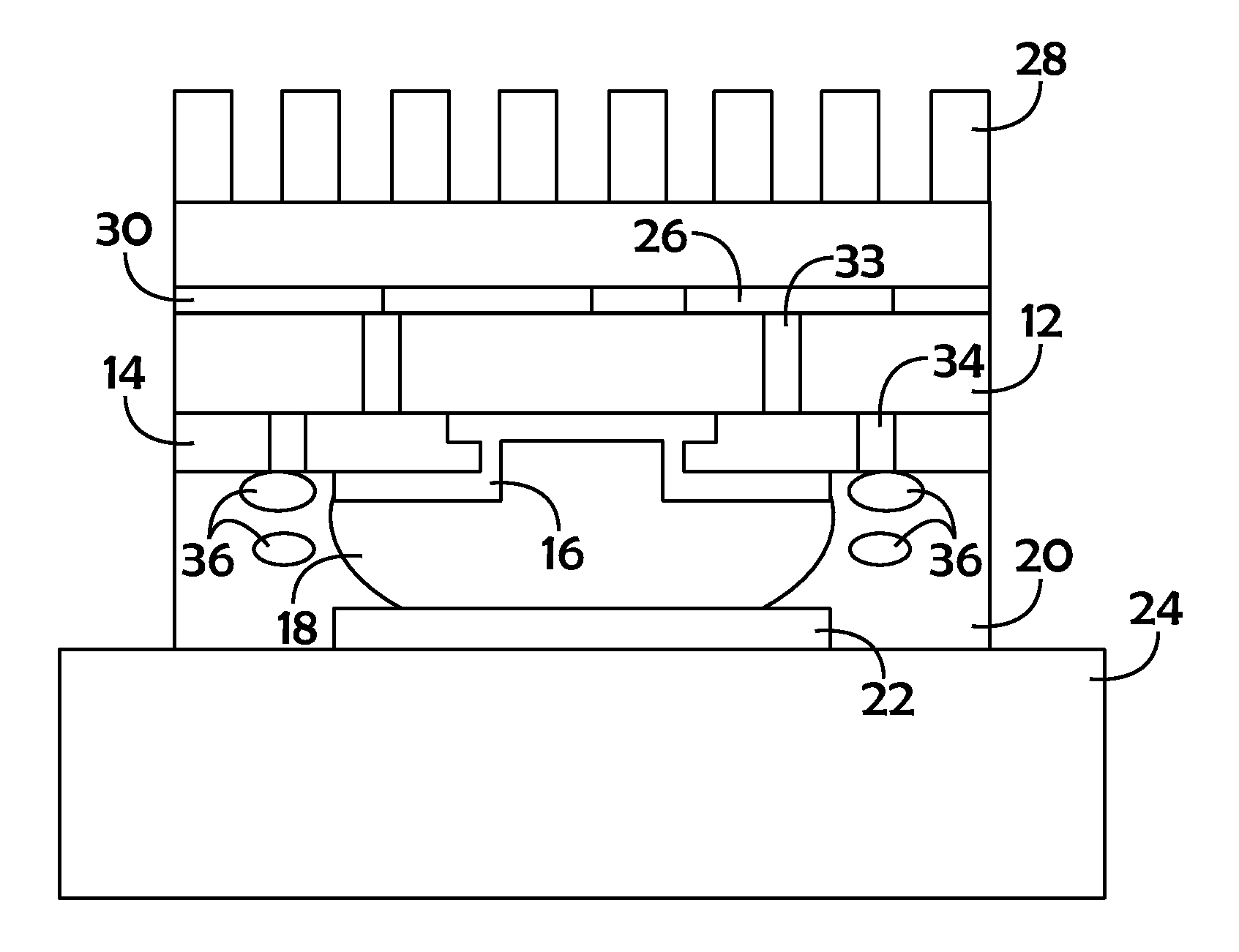
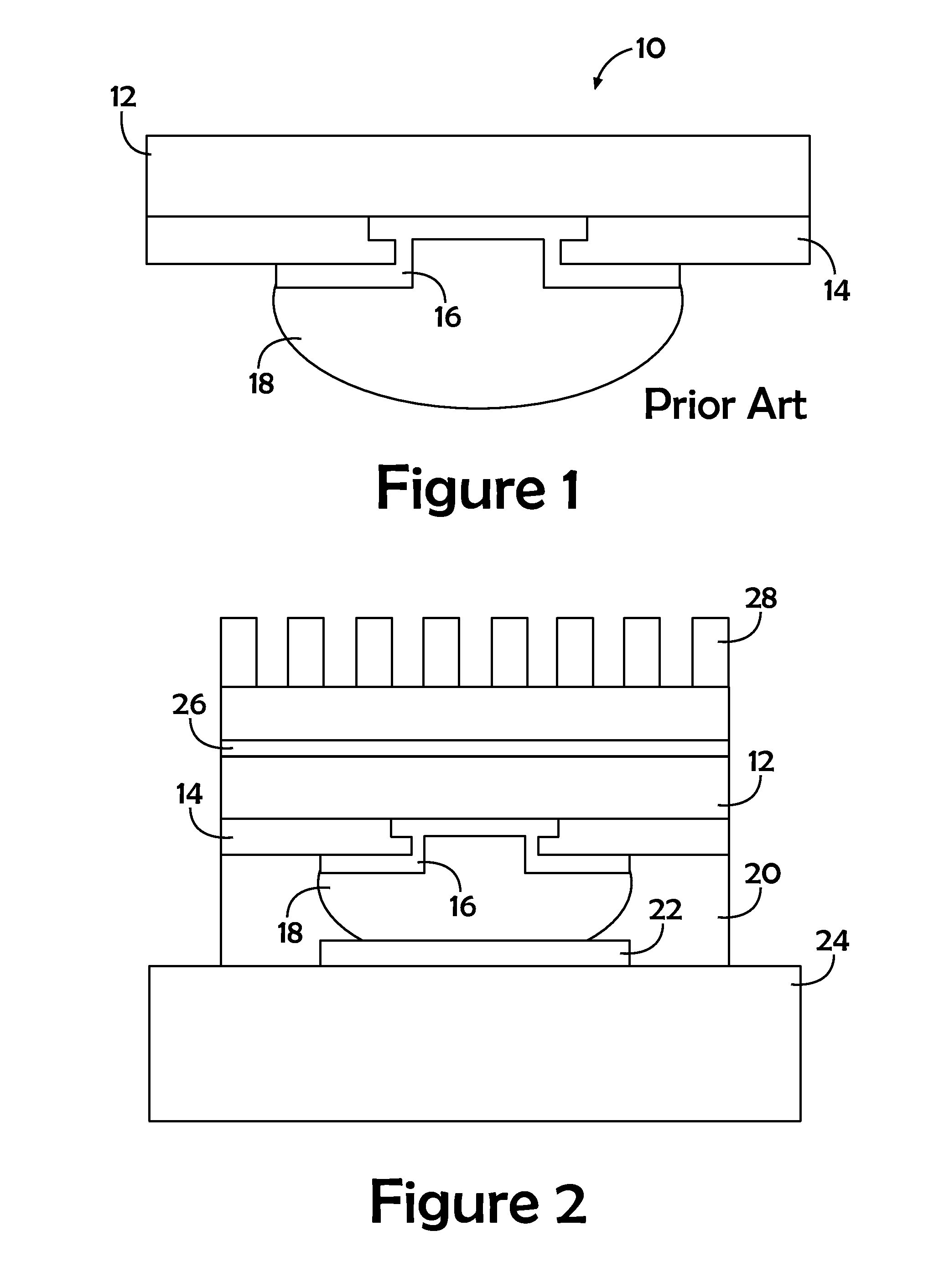
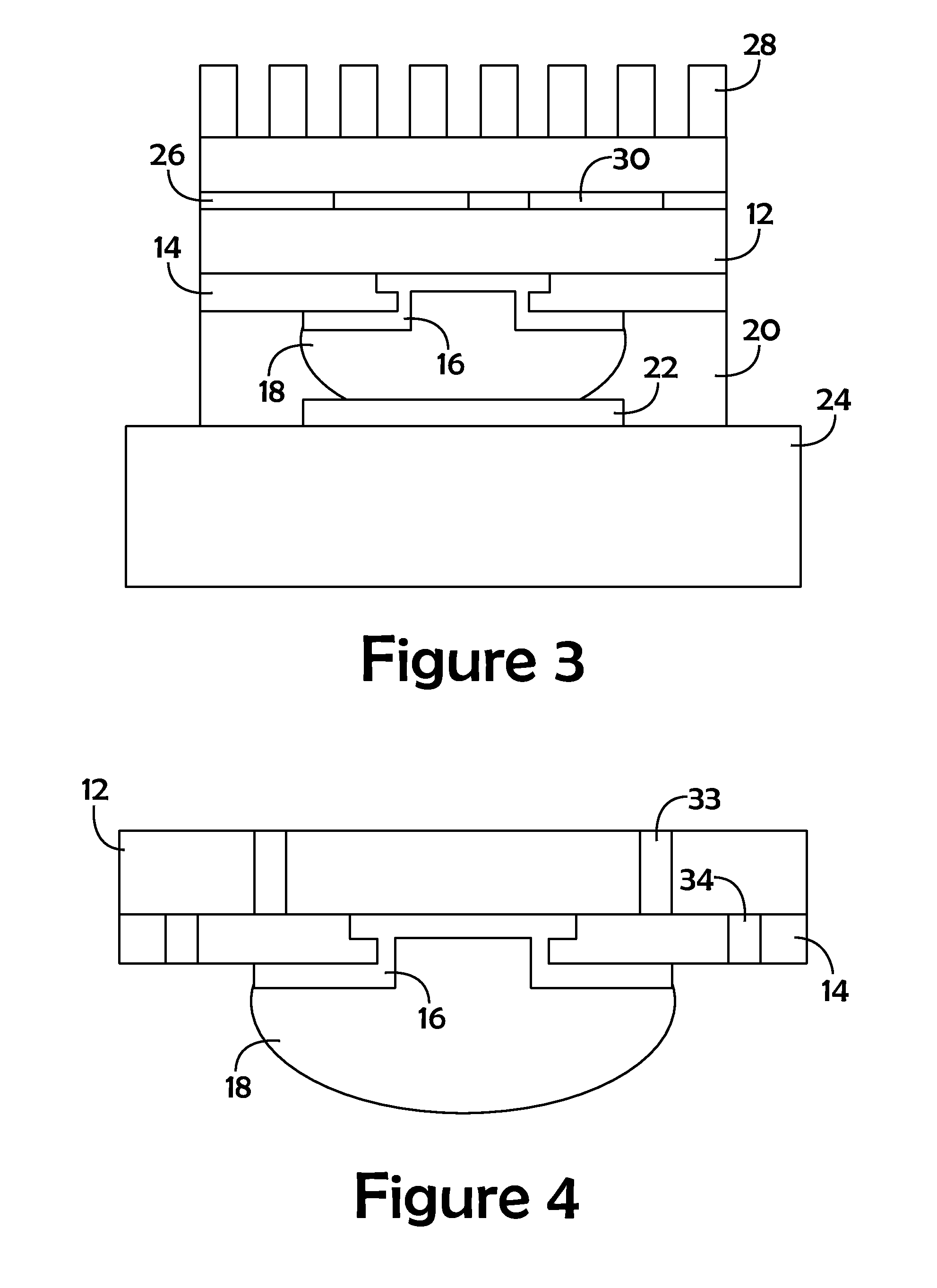
[0032]The present invention is a microchip package including fluid- or nanofluid-filled capsule, channel, or reservoir. When the package is compromised, the fluid destroys dies or circuitry on the chip.

[0033]An anti-tampering approach described herein uses the same chemical processes to remove the chip trace that is left over from the manufacturing process. Because the protective coating is no longer present on the chip, the bare chip trace is susceptible to etching in the same respect as the original conductive or semi-conductive deposition layer during the manufacturing process. Release of etchants onto the bare chip surface, therefore, will compromise the chip architecture as well as the memory and software stored on the chip.

[0034]Chip traces may also be damaged if an excessive amount of heat is applied to the chip. Heat may be generated by mixing a variety of two or more chemicals that will react together to create an exotherm. As can be appreciated by one skilled in the art, a...


PUM


Abstract

A tamper-resistant microchip package contains fluid- or nanofluid-filled capsules, channels, or reservoirs, wherein the fluids, either alone or in combination, can destroy circuitry by etching, sintering, or thermally destructing when reverse engineering of the device is attempted. The fluids are released when the fluid-filled cavities are cut away for detailed inspection of the microchip. Nanofluids may be used for the sintering process, and also to increase the thermal conductivity of the fluid for die thermal management. Through-vias and micro vias may be incorporated into the design to increase circuitry destruction efficacy by improving fluid/chip contact. Thermal interface materials may also be utilized to facilitate chip cooling.

Description

FIELD OF THE INVENTION[0001]The present invention relates to tamper-resistant microchip technology and, more particularly, to microchip packages comprising fluid- or nanofluid-filled capsules, channels, or reservoirs in which fluid released during a tampering event will destroy dies or circuitry via etching, sintering, or thermal destruction.BACKGROUND OF THE INVENTION[0002]The development of microelectronic circuitry is presently one of the most active areas of technological advancement, and therefore demands substantial economic and infrastructure resources. To recoup their investment and maintain a competitive position in the marketplace, microelectronic device manufacturers strive to protect their cutting-edge technologies from unauthorized disclosure. Once the development of microelectronic components reaches the manufacturing stage, however, and the devices are distributed to customers or otherwise fall into the hands of third parties, manufacturers lose a great deal of contro...

Claims


Application Information

Patent Timeline
IPC IPC(8): H01L23/22
CPCH01L23/42H01L2224/2929H01L24/13H01L24/16H01L24/29H01L2224/13101H01L2224/16225H01L2224/73204H01L2224/73253H01L2924/01013H01L2924/01029H01L2924/0103H01L2924/01047H01L2924/01079H01L23/573H01L2224/29101H01L2924/0665H01L2924/014H01L2924/01078H01L2924/01072H01L2924/01033H01L2924/01024H01L2924/01019H01L2924/01006H01L2224/29339H01L2224/29344H01L2224/29369H01L2224/29387H01L2224/29393H01L2924/10253H01L2224/29H01L2224/2919H01L2924/01005H01L2924/00H01L2924/00014H01L2924/14
Inventor DAS, RABINDRA N.MARKOVICH, VOYA R.MCNAMARA, JR., JAMES J.POLIKS, MARK D.
Owner I3 ELECTRONICS
Why Eureka
Try Eureka