Liquid crystal display device

a liquid crystal display and display device technology, applied in non-linear optics, instruments, optics, etc., can solve the problems of insufficient inability to prevent moisture intrusion, and inability to ensure the bonding strength of sealan

Active Publication Date: 2012-03-29
JAPAN DISPLAY INC +1
View PDF11 Cites 11 Cited by
  • Summary
  • Abstract
  • Description
  • Claims
  • Application Information

AI Technical Summary

Benefits of technology

[0024]According to the first means of the invention, when optical alignment is performed using ultraviolet light, the ultraviolet light is not radiated directly to the overcoat film so that the overcoat film is not deteriorated, which can prevent intrusion of moisture from the deteriorated portion of the overcoat film.
[0025]According to the second means of the invention, in the seal portion on the side where the counter substrate is formed, the sealant is bonded to the alignment film at part of the seal portion, and the sealant at another part of the seal portion is bonded to the overcoat film. When optical alignment is performed, the overcoat film is deteriorated at the portion where the sealant is in direct contact with the overcoat film. However, since the moisture is blocked at a portion where the sealant is bonded to the alignment film, intrusion of the moisture can be prevented. In contrast, since a portion where the sealant is bonded to the overcoat film is also present, the bonding strength of the sealant can also be ensured sufficiently.
[0026]According to the third means of the invention, since, also on the side of the TFT substrate, a portion of the sealant is in contact with the alignment film and other portion thereof is in contact with the inorganic insulating film, prevention for the moisture intrusion and reliability for the seal portion can be attained simultaneously. At the same time, since an identical printing plate can be used for the counter substrate and the TFT substrate when the alignment film is printed, manufacturing cost of the liquid crystal display panel can be decreased.

Problems solved by technology

However, if the ultraviolet light is radiated to a portion other than the alignment film, the radiated portion is deteriorated by the ultraviolet light to result in a problem.
Such a problem is particularly significant when the material radiated by the ultraviolet light is an organic material.
FIG. 8 is a cross sectional view of a seal portion that is included in a liquid crystal display panel having a conventional structure, which shows a problem occurring when optical alignment is performed on an alignment film 113.

Method used


Image

  • Liquid crystal display device
  • Liquid crystal display device
  • Liquid crystal display device

Examples


example 1

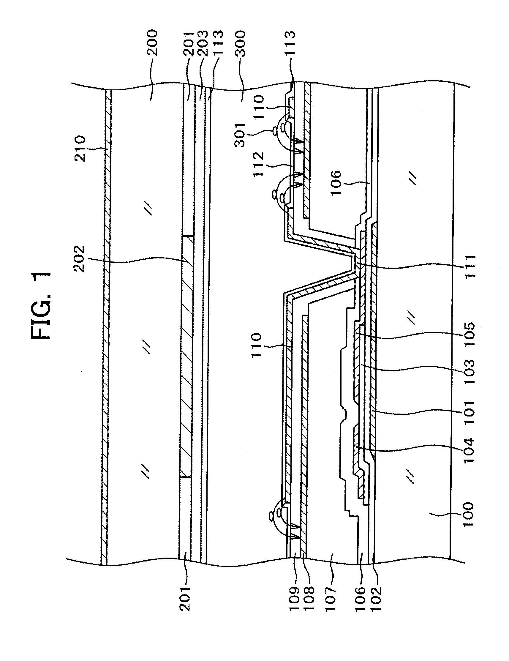
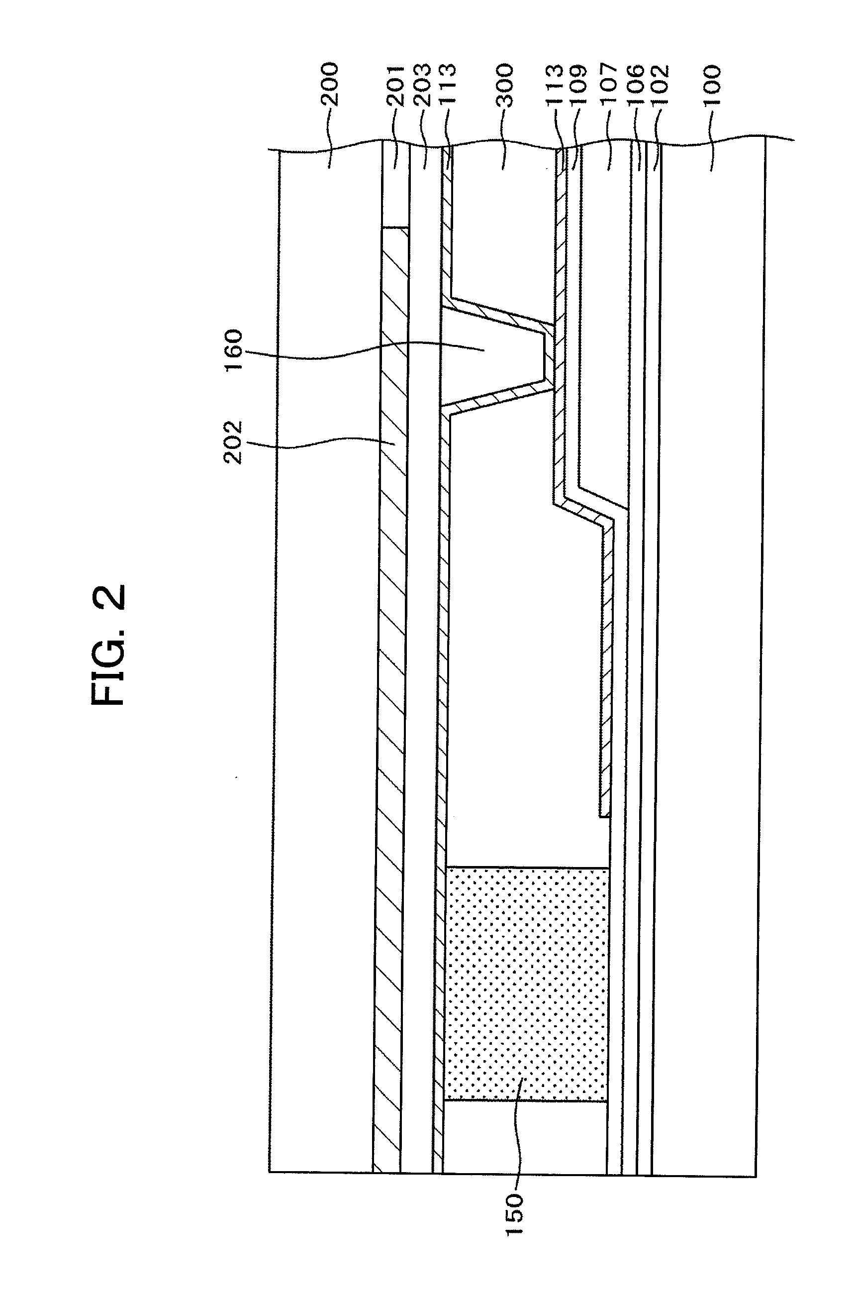
[0049]FIG. 2 is a cross sectional view of a seal portion of the liquid crystal display panel in this example and this is a cross sectional view of the seal portion of the IPS liquid crystal display panel described with reference to FIG. 1. In FIG. 2, the external conductive film formed on the side of the counter substrate 200 is not illustrated.

[0050]In FIG. 2, a gate insulating film 102, an inorganic passivation film 106, an organic passivation film 107, an interlayer insulating film 109, and an alignment film 113 are stacked on a TFT substrate 100. The organic passivation film 107 is for planarizing the display region and not extended as far as the seal portion. The interlayer insulating film 109 formed on the organic passivation film 107 extends as far as the end of the TFT substrate 100. The alignment film 113 is formed covering the interlayer insulating film 109.

[0051]A color filter 201 and a black matrix 202 and an over coat film 203 are formed on the side where the counter su...

example 2

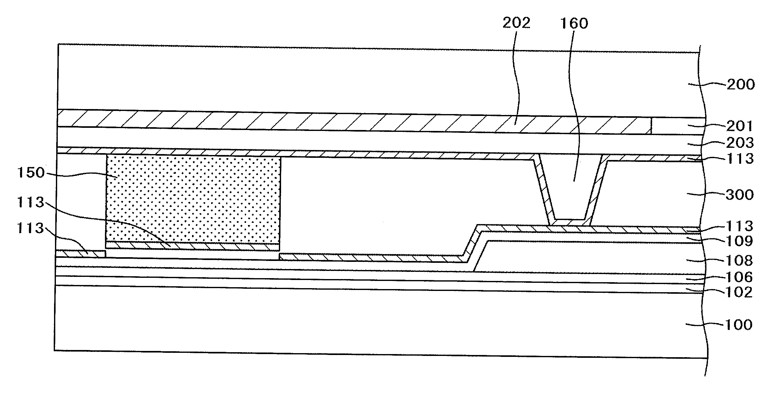
[0056]FIG. 3 is a cross sectional view showing a second example according to the invention. In FIG. 3, description for the structure identical with that in FIG. 2 is omitted. In the counter substrate 200 of FIG. 3, while the alignment film 113 is formed for the display region and at the end of the counter substrate 200, the alignment film 113 is not formed at the portion where the sealant 150 is formed except for the end of the counter substrate 200.

[0057]When optical alignment is performed on the counter substrate 200 as described above, the overcoat film 203 at the portion not covered with the alignment film 113 is deteriorated by the ultraviolet light. However, since a portion A where the alignment film 113 is formed overlapping the portion formed with the sealant 150 is present, deterioration of the overcoat film 203 is not caused in the portion A. Accordingly, since moisture from the outside is blocked at the portion A, the inside of the liquid crystal display panel is protecte...

example 3

[0062]FIG. 5 is a cross sectional view showing a third example according to the invention. FIG. 5 is different from FIG. 3 in the structure of the TFT substrate 100 in the seal portion. In the TFT substrate 100 of FIG. 5, while the alignment films 113 is formed in the display region and at the end of the counter substrate 200, the alignment film 113 is not formed at the portion where the sealant 150 is formed except for the outer side. That is, in FIG. 5, the range over which the alignment film 113 extends on the side of the TFT substrate 100 is identical with that on the side of the counter substrate 200.

[0063]The alignment film 113 is generally formed by flexographic printing. When the range over which the alignment film 113 extends on the side of the counter substrate 200 is identical with that on the side of the TFT substrate 100, one printing plate will suffice. In contrast, in Example 1 and Example 2, two flexographic printing plates are necessary for the TFT substrate 100 and...


PUM

PropertyMeasurementUnit
thicknessaaaaaaaaaa
humidityaaaaaaaaaa
temperatureaaaaaaaaaa

Abstract

A liquid crystal display device includes a TFT substrate having a first alignment film formed on part of an inorganic insulating film, an overcoat film formed on a black matrix, a counter substrate having a second alignment film formed on the overcoat film, and a seal portion including a sealant. The TFT substrate is bonded to the counter substrate by the sealant. The sealant is bonded to the inorganic insulating film at the seal portion on the side where the TFT substrate is formed, with the first alignment film not being provided on the side, and, in the seal portion on the side where the counter substrate is formed, the sealant is bonded to the second alignment film but, is not bonded to the overcoat film.

Description

CLAIM OF PRIORITY[0001]The present application claims priority from Japanese Patent Application JP 2010-217063 filed on Sep. 28, 2010, the content of which is hereby incorporated by reference into this application.BACKGROUND OF THE INVENTION[0002]1. Field of the Invention[0003]The present invention relates to a display device. The invention particularly relates to an IPS liquid crystal display device in which the reliability of a seal portion is improved.[0004]2. Description of the Related Art[0005]A liquid crystal display device includes a TFT substrate having pixel electrodes, thin film transistors (TFT), or the like formed thereon in a matrix form, and a counter electrode opposing the TFT substrate and having color filters, or the like formed at positions corresponding to the pixel electrodes of the TFT substrate. Liquid crystal is put between the TFT substrate and the counter substrate. The liquid crystal display device controls light transmittance for each pixel by using liquid...

Claims


Application Information

Patent Timeline
Patent Type & Authority Applications(United States)
IPC IPC(8): G02F1/1335
CPCG02F1/1339G02F2001/133519G02F1/133788G02F1/133519G02F1/1337G02F1/1368
Inventor SONODA, HIDEHIROKUNIMATSU, NOBORUMATSUI, CHIKAEYAMAMOTO, TAKASHI
Owner JAPAN DISPLAY INC
Why Eureka
Try Eureka