Semiconductor device

a technology of semiconductor devices and semiconductor components, applied in semiconductor devices, semiconductor/solid-state device details, electrical apparatus, etc., can solve the problems of dispersed distortion applied to external terminals in secondary packaging, falling of reliability in packaging semiconductor devices on printed boards, etc., to reduce the occurrence of fractures, improve the reliability of secondary packaging, and reduce distortion

Inactive Publication Date: 2012-04-12
PS4 LUXCO SARL
View PDF6 Cites 62 Cited by
  • Summary
  • Abstract
  • Description
  • Claims
  • Application Information

AI Technical Summary

Benefits of technology

[0009]Since the semiconductor device is configured as explained above, it is possible to prevent a warp that occurs in a boundary area because of the difference in the modulus of elasticity between an applied area of the bonding member and an area without the bonding member from occurring in an area where the bonding member overlaps external terminals such as solder balls. Consequently, distortion applied to the external terminals in secondary packaging is dispersed. This makes it possible to reduce occurrence of fracture in external terminal connecting sections an

Problems solved by technology

As a result, reliability in packaging the semiconductor device on a printed board (hereinafter referred to as second

Method used


Image

  • Semiconductor device
  • Semiconductor device
  • Semiconductor device

Examples


first exemplary embodiment

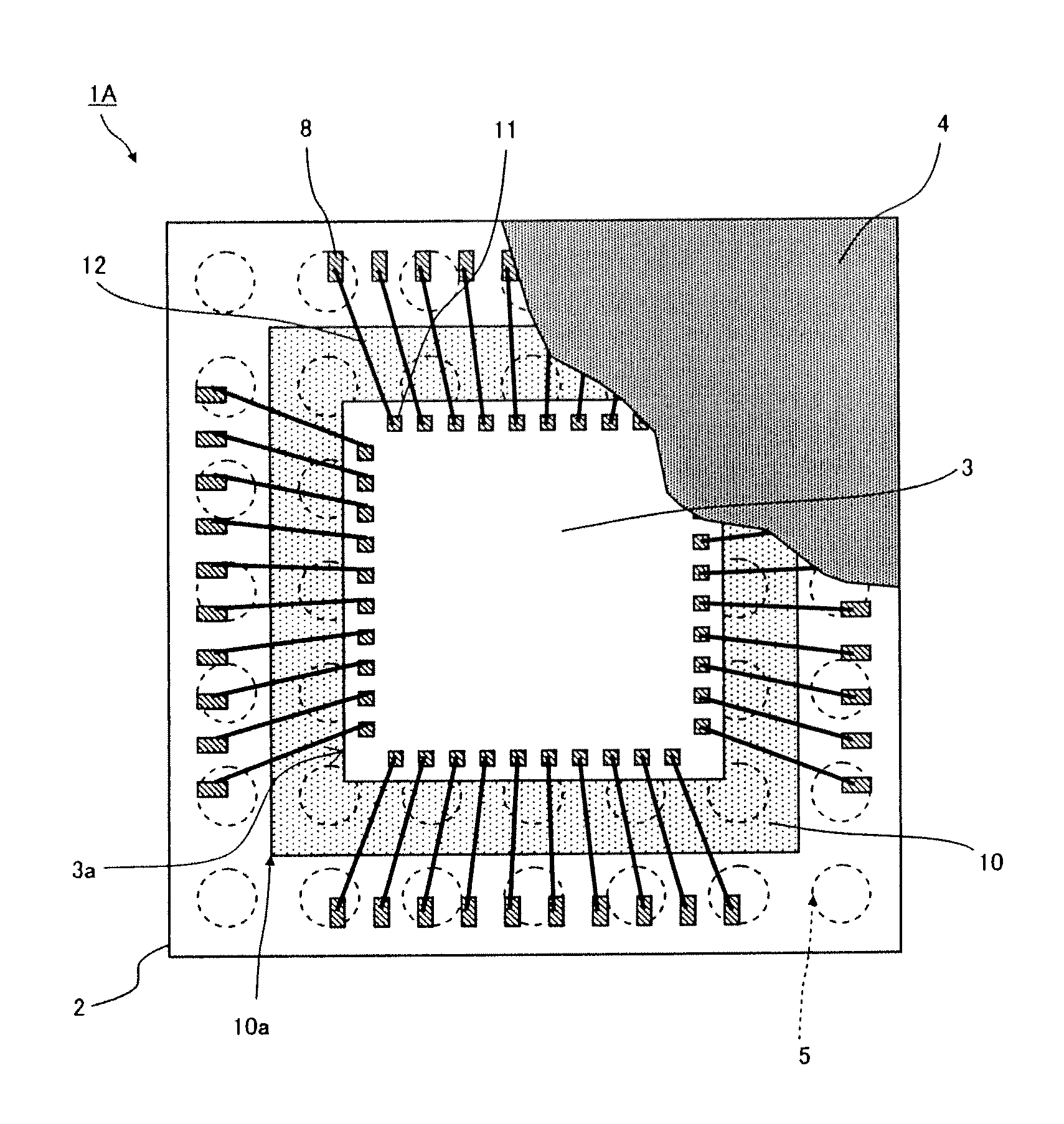
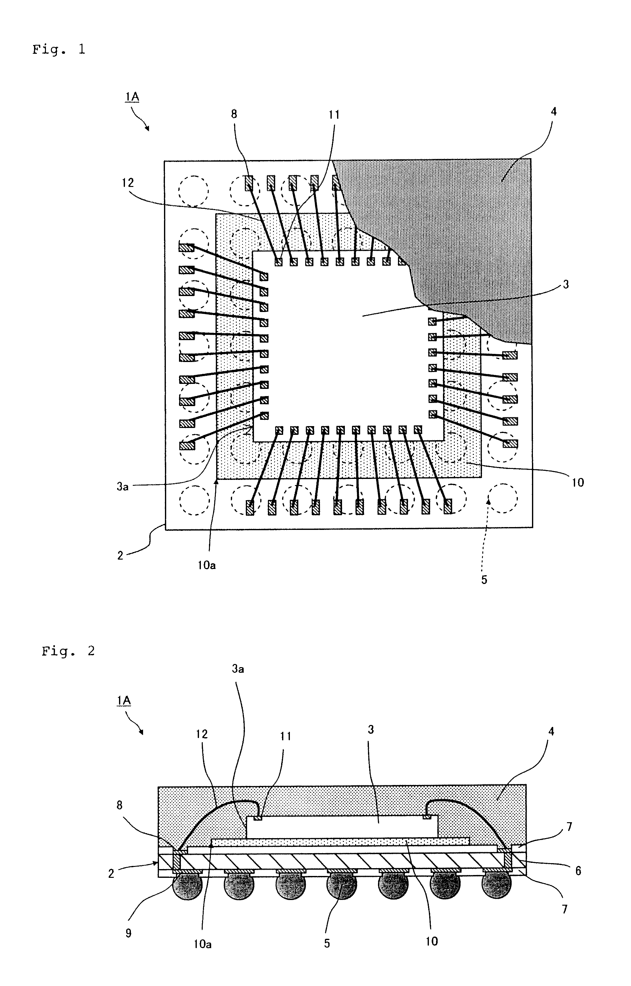
[0024]FIG. 1 is a plan view showing a schematic configuration of a semiconductor device according to a first exemplary embodiment. FIG. 2 is a sectional view of the schematic configuration.

[0025]Semiconductor device 1A according to this exemplary embodiment shown in FIGS. 1 and 2 includes wiring board 2 on one surface of which a predetermined wiring pattern (not shown) is formed, semiconductor chip 3 mounted on one surface of wiring board 2, sealing member 4 that covers the periphery of semiconductor chip 3 and that seals an electric connection section between semiconductor chip 3 and wiring board 2, and metal balls such as solder balls 5, which are external terminals, disposed on the other surface of wiring board 2. In FIG. 1, sealing member 4 is partially removed to clearly show the structure.

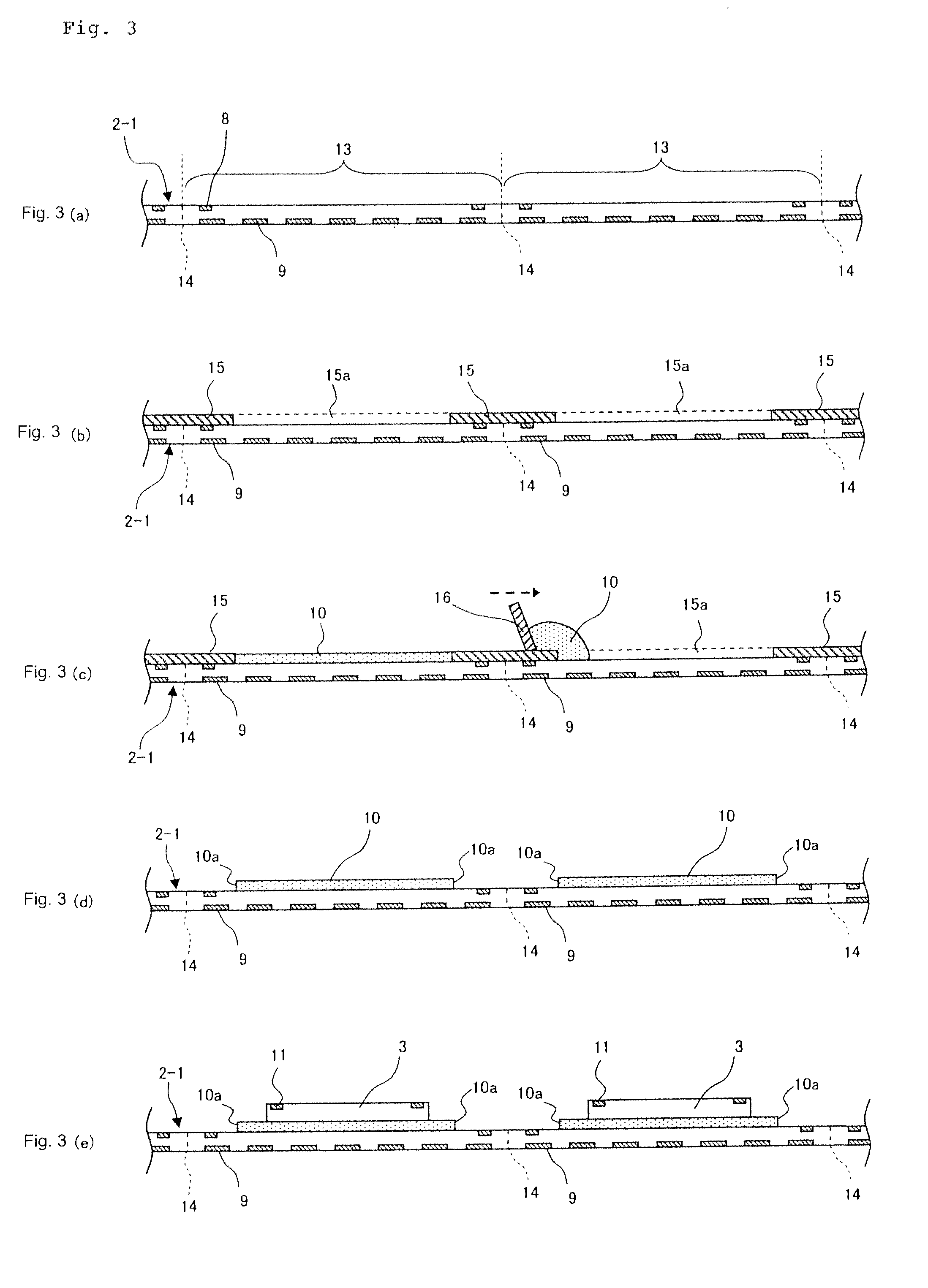
[0026]Wiring board 2 is formed by dividing, for each of plural product forming sections, a substantially rectangular glass epoxy wiring board (hereinafter referred to as wiring motherboard) i...

second exemplary embodiment

[0043]A second exemplary embodiment is explained below. Components that are the same as those in the first exemplary embodiment are denoted by the same reference numerals and signs. FIG. 5 is a plan view showing a schematic configuration of a semiconductor device according to the second exemplary embodiment. FIG. 6 is a sectional view of the schematic configuration.

[0044]Semiconductor device 1B according to this exemplary embodiment shown in FIGS. 5 and 6 includes wiring board 2 having opening 2a formed in the center, semiconductor chip 3 mounted on one surface of wiring board 2, sealing member 4 that covers the periphery of semiconductor chip 3 and that seals an electric connection section of semiconductor chip 3 and wiring board 2 in opening 2a, and metal balls of solder balls 5, which are external terminals, disposed on the other surface of wiring board 2. In FIG. 5, sealing member 4 is partially removed to clearly show the structure.

[0045]Wiring board 2 is formed by dividing, fo...

third exemplary embodiment

[0062]A third exemplary embodiment is explained below. Components that are the same as those in the first exemplary embodiment are denoted by the same reference numerals and signs. FIG. 9 is a plan view showing a schematic configuration of a semiconductor device according to the third exemplary embodiment. FIG. 10 is a sectional view of the schematic configuration.

[0063]Semiconductor device 1C according to this exemplary embodiment shown in FIGS. 9 and 10 is configured substantially the same as semiconductor device 1B according to the second exemplary embodiment. However, semiconductor device 1C is different from semiconductor device 1B in that bonding members 10 are formed over substantially the entire surface on the one surface side of wiring board 2. Specifically, peripheral ends 10a of bonding members 10 spread from the edges of opening 2a to the vicinities of outer peripheral end 2b of wiring board 2. Consequently, peripheral ends 10a of bonding members 10 are arranged on the o...


PUM


Abstract

The present invention reduces the occurrence of fracture in external terminal connecting sections and improves the reliability of secondary packaging of a semiconductor device. Specifically, the present invention provides a semiconductor device including a wiring board, a semiconductor chip mounted on one surface of the wiring board via a bonding member, and external electrodes formed on the other surface of the wiring board and electrically connected to the semiconductor chip. In the semiconductor device, a peripheral end of the bonding member is arranged in a position where the peripheral end does not overlap the external electrodes.

Description

[0001]This application is based upon and claims the benefit of priority from Japanese patent application No. 2010-229615, filed on Oct. 12, 2010 and Japanese patent application No. 2010-280391, filed on Dec. 16, 2010, the disclosure of which are incorporated herein in its entirety by reference.BACKGROUND OF THE INVENTION[0002]1. Field of the Invention[0003]The present invention relates to a semiconductor device in which a semiconductor chip is mounted on one surface of a wiring board and plural external terminals are arranged in a grid shape on the other surface of the wiring board.[0004]2. Description of Related Art[0005]JP2001-044324A and JP2001-044229A disclose a semiconductor device in which a semiconductor chip is mounted on one surface of a wiring board via a bonding member and solder balls electrically connected to the semiconductor chip are disposed on the other surface of the wiring board. The semiconductor device of this type is called a BGA (Ball Grid Array) type semicond...

Claims


Application Information

Patent Timeline
IPC IPC(8): H01L25/07H01L23/495
CPCH01L21/561H01L21/6836H01L23/13H01L23/3128H01L23/49816H01L24/27H01L24/32H01L24/48H01L24/83H01L24/97H01L25/0657H01L2221/68327H01L2224/06156H01L2224/2732H01L2224/29099H01L2224/32145H01L2224/32225H01L2224/48091H01L2224/48227H01L2224/4824H01L2224/48463H01L2224/49171H01L2224/73215H01L2224/73265H01L2224/83192H01L2224/85203H01L2224/92147H01L2224/95H01L2224/97H01L2924/01029H01L2924/01079H01L2924/014H01L2924/15311H01L2224/2919H01L2924/01005H01L2924/01006H01L2924/01033H01L2924/0665H01L24/29H01L24/743H01L24/49H01L21/565H01L24/45H01L24/73H01L2224/04042H01L2224/06155H01L2224/45144H01L2224/45147H01L2224/85205H01L2225/0651H01L2924/1431H01L2924/1434H01L2225/06568H01L2224/32013H01L24/14H01L2224/85H01L2224/83H01L2924/00014H01L2224/92247H01L2924/00H01L2924/00012H01L2924/3512H01L2924/181H01L2224/05554H01L2224/85399H01L2224/05599
Inventor IWAMOTO, YOSHINORISATO, KOUJINAKAJIMA, YUTAKAHAYAKAWA, KEN
Owner PS4 LUXCO SARL
Why Eureka
Try Eureka