Pixel circuit and display panel with ir-drop compensation function

a pixel circuit and display panel technology, applied in the field of pixel circuits and display panels, can solve the problem that the real work voltage actually transmitted to the multiple pixel circuits from the current supply line i cannot be fixed at ovdd

Inactive Publication Date: 2012-04-12
AU OPTRONICS CORP
View PDF12 Cites 56 Cited by
  • Summary
  • Abstract
  • Description
  • Claims
  • Application Information

AI Technical Summary

Benefits of technology

[0017]In the pixel circuit and the display panel with the IR-drop function of the present invention, the effect of the line resistance of the current-supply line on the current flowing through the current-driven device can be eliminated through compensating the data at the data line by a difference value between the real work voltage and the original work voltage.

Problems solved by technology

However, because the current-supply line I has a line resistance which may cause an IR-drop, the real work voltage actually transmitted to the multiple pixel circuits from the current-supply line I can not be fixed at OVDD.

Method used


Image

  • Pixel circuit and display panel with ir-drop compensation function
  • Pixel circuit and display panel with ir-drop compensation function
  • Pixel circuit and display panel with ir-drop compensation function

Examples


Embodiment Construction

[0025]The present invention will now be described more specifically with reference to the following embodiments. It is to be noted that the following descriptions of preferred embodiments of this invention are presented herein for purpose of illustration and description only. It is not intended to be exhaustive or to be limited to the precise form disclosed.

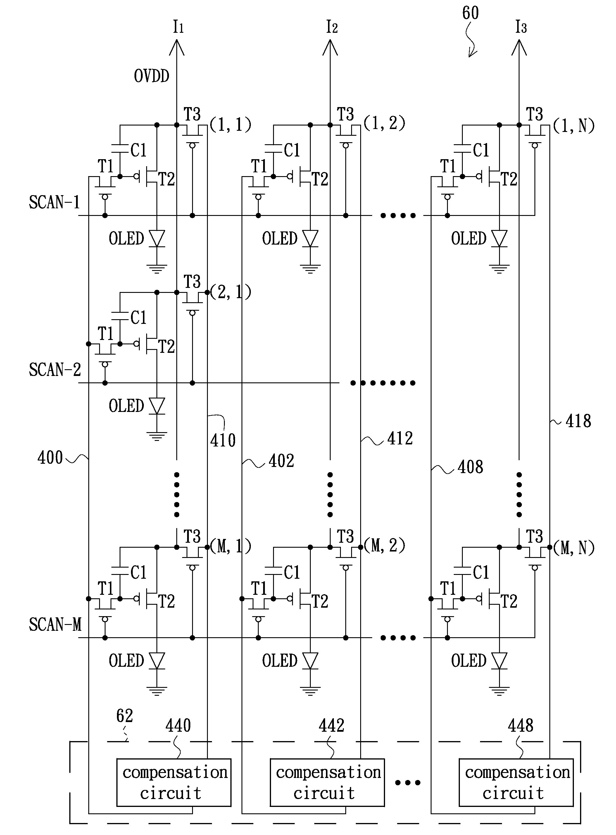
[0026]FIG. 4 is a circuit diagram of a LED display panel with an IR-drop compensation function in an embodiment of the present invention. As depicted in FIG. 4, the LED display panel 60 includes multiple data lines 400, 402 . . . 408, multiple control lines SCAN-1, SCAN-2 . . . SCAN-M, multiple power-supply lines I, I2 . . . I3, multiple compensation circuits 440, 442 . . . 448 and multiple pixel circuits (1,1), (1,2) . . . (M,N). As depicted in FIG. 4, the control ends of both the first transistor switches T1 and the detecting switches T3 of the N pixel circuits, such as, (1,1), (1,2) . . . (1,N) in a same row, are electrically ...


PUM


Abstract

A pixel circuit and a display panel with an IR-drop compensation function are disclosed. The display panel includes multiple pixel circuits and multiple compensation circuits. Each of the pixel circuits includes a detecting switch. After a real work voltage of a pixel circuit is transmitted to a corresponding compensation circuit through a corresponding detecting switch, a data transmitted to the pixel circuit is adjusted by the compensation circuit according to a relationship between the real work voltage and an original work voltage.

Description

FIELD OF THE INVENTION[0001]The present invention relates to pixel circuits and display panels, and more particularly to a pixel circuit and a display panel with an IR-drop (internal-resistance drop) compensation function.BACKGROUND OF THE INVENTION[0002]OLEDs (Organic light emitting diode) have characteristics of thin thickness, light weight, self-illumination, low drive voltage, high efficiency, high contraction, high color saturation and high response speed. After the TFT (Thin Film Transistor), the OLEDs are known as the most promising and new display technique.[0003]FIG. 1 is a diagram of a conventional OLED display 10. The OLED display 10 includes N*M pixel circuits which are electrically coupled to a current-supply line I from which an original work voltage OVDD can be supplied to each of the N*M pixel circuits. Moreover, the N pixel circuits arranged in a same row are electrically coupled to a same control line; for example, the N pixel circuits (1,1), (1,2), . . . , (1,N) i...

Claims


Application Information

Patent Timeline
Patent Type & Authority Applications(United States)
IPC IPC(8): G09G5/00
CPCG09G3/3233G09G3/3275G09G2320/0233G09G2300/0842G09G2320/0223G09G2300/0819
Inventor TSENG, SZU-HENGTSAI, TZE-CHIEN
Owner AU OPTRONICS CORP
Why Eureka
Try Eureka