
Capacitive touch screen having dynamic capacitance control and improved touch-sensing

a capacitance control and capacitance control technology, applied in the field of capacitance touch sensing screens, can solve the problems of unavoidable and usually unwanted capacitance, and achieve the effect of affecting the capacitance of the touch sensing pad, sensitivity and performan

Inactive Publication Date: 2012-04-19
UICO
View PDF9 Cites 56 Cited by
  • Summary
  • Abstract
  • Description
  • Claims
  • Application Information

AI Technical Summary

Benefits of technology

[0011]In another embodiment of the invention, EMCS can be implemented as other touch sensing pads that can be electrically manipulated. When this is done, time multiplexing of a plurality of touch sensing pads as sensors or EMCS yields similar results and allows precise tuning of the natural capacitance of each touch sensing pad. Each conductive pad is charged and monitored for rate of discharge in a predetermined sequence as touch is sensed. Inactive pads that are not being used for touch sensing and that are adjacent to the active sensing pad can be used as EMCS by controlling their charge level relative to the active sensing pad. Effective use of EMCS enables the ability to adjust the relative charge and capacitance of the touch sensing pads dynamically and to optimize it for desired performance.
[0023]According to an embodiment of the invention, a method of improving the sensing performance of a capacitive touch screen device including at least one capacitive touch pad element, the method includes selectively altering a magnitude of an electrical potential of at least one electrically conductive structure proximate the at least one capacitive touch pad element based on an electrical potential of the at least one capacitive touch pad element, to alter an effective capacitance of the at least one capacitive touch pad element, and subsequently detecting a user touch of the at least one capacitive touch pad element. In an embodiment, the electrical potential of the at least one electrically conductive structure is altered to substantially match the electrical potential of the at least one capacitive touch pad element. In an alternative embodiment, the electrical potential of the at least one electrically conductive structure is altered to a magnitude substantially different from the electrical potential of the at least one capacitive touch pad element. The method may further include disposing a plurality of electrically conductive elements proximate the at least one capacitive touch pad element. The electrical potential of each of the plurality of electrically conductive elements may be altered based on the electrical potential of the at least one capacitive touch pad element. In another embodiment, the capacitive touch screen may includes a plurality of capacitive touch pad elements, and a plurality of electrically conductive elements may be disposed proximate each capacitive touch pad element of the plurality. The at least one electrically conductive element may be another capacitive touch pad element disposed proximate the at least one capacitive touch pad element.

Problems solved by technology

Parasitic capacitance is the unavoidable and usually unwanted capacitance that exists between the parts of an electronic component or circuit simply because of the proximity of conductive parts to each other.

Method used


Image

  • Capacitive touch screen having dynamic capacitance control and improved touch-sensing
  • Capacitive touch screen having dynamic capacitance control and improved touch-sensing
  • Capacitive touch screen having dynamic capacitance control and improved touch-sensing

Examples


Embodiment Construction

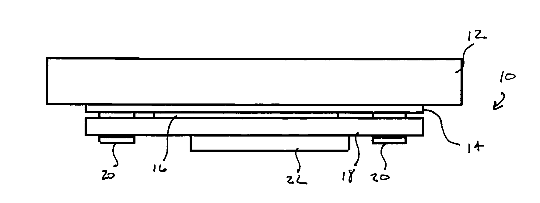
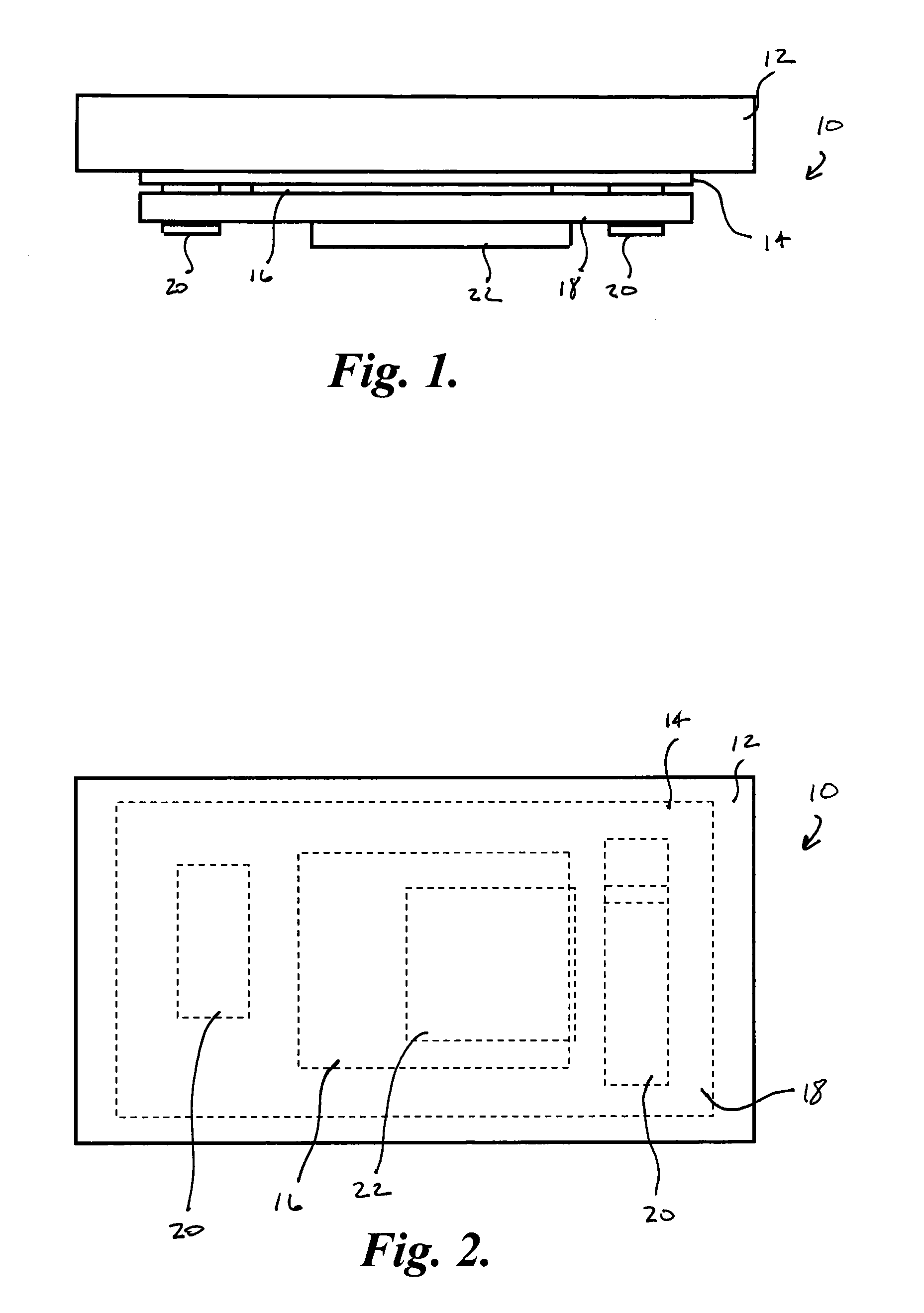
[0037]Referring to FIGS. 1 and 2, capacitive touch sensing screen device 10 generally includes substrate 12, adhesive 14, touch sensing screen 16, PCB substrate 18, traces 20 and a controlling processor in the form of integrated circuit 22. Processor 22 or other electronic components are coupled to traces 20 to control and manipulate the charge on structures of capacitive touch sensing screen 10 as is known in the art.

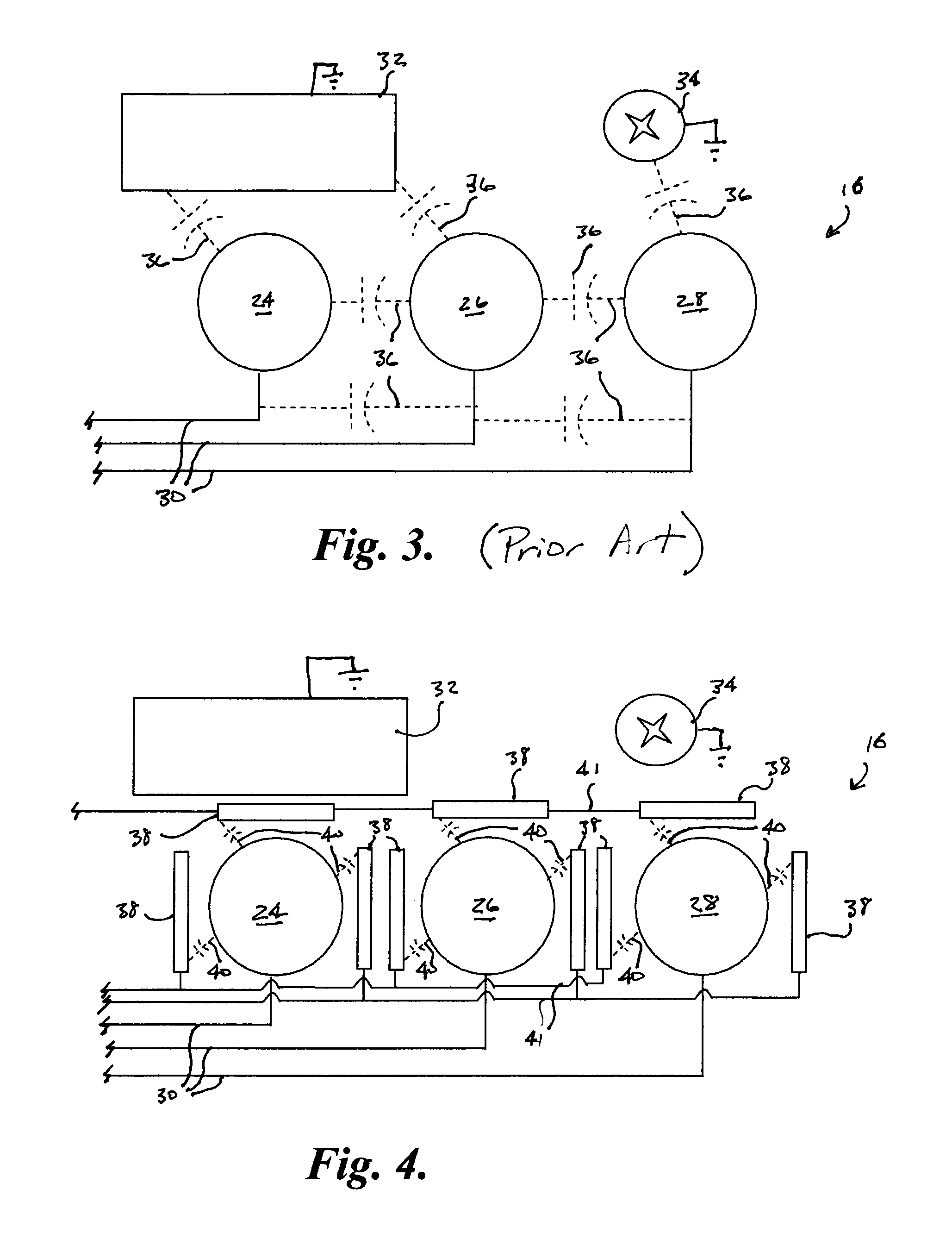
[0038]Referring now to FIG. 3, a typical prior art capacitive touch sensing screen 16 includes first touch pad 24, second touch pad 26, third touch pad 28, touch pad conductors 30 coupled to traces 20, metal bracket 32 and screw 34. Metal bracket 32 and screw 34 are generally at chassis ground potential. Parasitic capacitance 36 is depicted in FIG. 3. Parasitic capacitance 36 exists between various conductive parts of the circuit because of the proximity of conductive parts to each other. In FIG. 3, parasitic capacitance is depicted as existing between first touch pad ...


PUM


Abstract

Methods and apparatus for improving the sensing performance of a capacitive touch screen sensing device. The electrical potential of conductive structures proximate capacitive touch pads of the sensing device is altered to compensate for the effect of parasitic capacitance, based on external conditions such as water on the touch screen or an intervening user worn glove. The compensation for parasitic capacitance improves the signal to noise ratio and therefore the sensing performance of the device.

Description

RELATED APPLICATIONS[0001]This application claims the benefit of U.S. Provisional Patent Application No. 61 / 377,837, filed Aug. 27, 2010, and entitled CAPACITIVE TOUCH SCREEN HAVING DYNAMIC CAPACITANCE CONTROL AND IMPROVED TOUCH-SENSING, said application being hereby fully incorporated herein by reference.FIELD OF THE INVENTION[0002]The invention relates to capacitive touch sensing technologies. More specifically, the invention relates to capacitive touch sensing screens such as those used in mobile phones and other digital appliances.BACKGROUND OF THE INVENTION[0003]Touch screens are electronic visual displays that can detect the presence and location of a touch on the surface of the display area. Touching of the display is generally done with a finger or hand. Touch screens operate under a variety of electronic, acoustic or optical principals. This application is concerned with capacitive touch screens.[0004]Capacitive touch screen panels generally include an insulator, such as gl...

Claims


Application Information

Patent Timeline
Patent Type & Authority Applications(United States)
IPC IPC(8): G06F3/044
CPCG06F3/044G06F3/0418G06F3/04186
Inventor WADIA, BAHAR N.
Owner UICO
Learn More