Check patentability & draft patents in minutes with Patsnap Eureka AI!

Method of Manufacturing Organic Light Emitting Display Apparatus, and Organic Light Emitting Display Apparatus Manufactured by Using the Method

Inactive Publication Date: 2012-04-26
SAMSUNG DISPLAY CO LTD
View PDF6 Cites 40 Cited by
  • Summary
  • Abstract
  • Description
  • Claims
  • Application Information

AI Technical Summary

Benefits of technology

[0008]Exemplary embodiments according to the present invention provide a method of manufacturing an organic light-emitting display device that is suitable for manufacturing l

Problems solved by technology

However, the deposition method using such FMM is not suitable for manufacturing larger devices using a mother glass having a size of 5 G or greater.
For instance, when such a large mask is used, the mask may bend due to its own weight, thereby distorting a pattern.
This is not conducive for the recent trend towards high-definition patterns.

Method used


Image

  • Method of Manufacturing Organic Light Emitting Display Apparatus, and Organic Light Emitting Display Apparatus Manufactured by Using the Method
  • Method of Manufacturing Organic Light Emitting Display Apparatus, and Organic Light Emitting Display Apparatus Manufactured by Using the Method
  • Method of Manufacturing Organic Light Emitting Display Apparatus, and Organic Light Emitting Display Apparatus Manufactured by Using the Method

Examples


Embodiment Construction

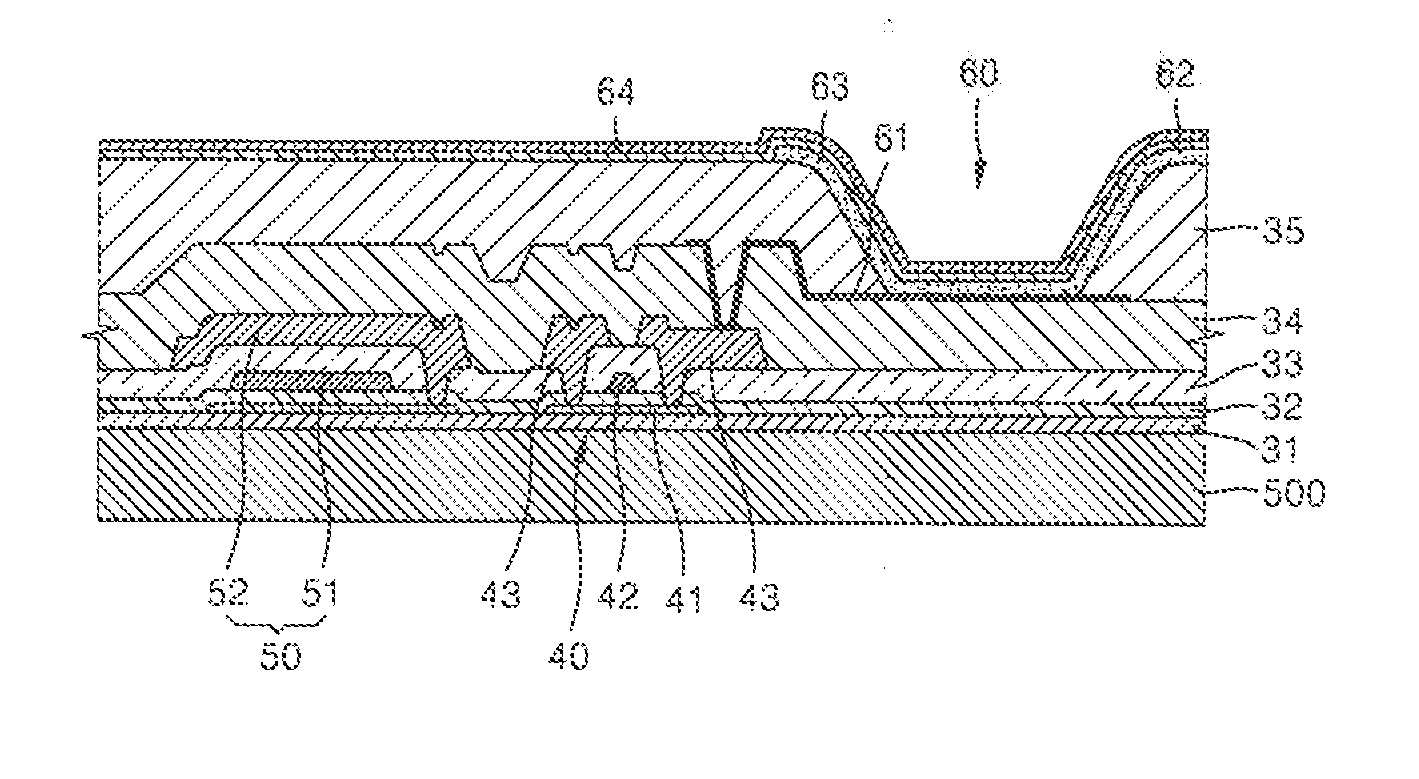
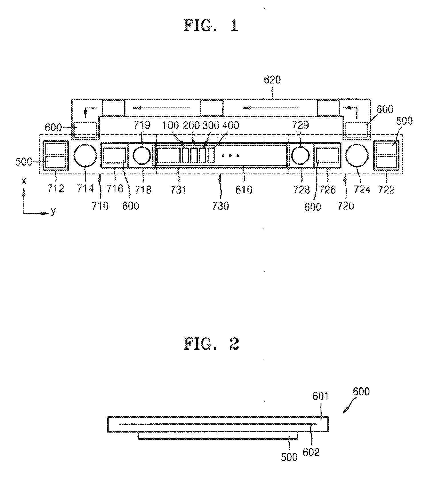
[0045]Reference will now be made in detail to embodiments, examples of which are illustrated in the accompanying drawings. In this regard, the embodiments described herein may be modified to have different forms and should not be construed as being limited to the descriptions set forth herein. FIG. 1 is a schematic view of an organic layer deposition apparatus according to an embodiment of the present invention.

[0046]Referring to FIG. 1, the thin film deposition apparatus (e.g., organic layer deposition apparatus) according to one embodiment includes a loading unit 710, a deposition unit 730, an unloading unit 720, a first conveyer unit 610, and a second conveyer unit 620.

[0047]The loading unit 710 may include a first rack 712, a transport robot 714, a transport chamber 716, and a first inversion chamber 718.

[0048]A plurality of substrates 500 onto which a deposition material is to be applied are stacked up on the first rack 712. The transport robot 714 picks up one of the substrate...


PUM


Abstract

A method of manufacturing an organic light emitting display device and an organic light emitting display device manufactured using the method, which are suitable for manufacturing large-sized display devices on a mass scale and can be used for high-definition patterning. The method includes consecutively forming organic layers on a substrate on which a plurality of panels are arranged parallel to each other; forming a second electrode on the organic layers, for each of the panels; forming a passivation layer on the second electrode on each of the panels to cover the second electrode; and removing a part of the organic layers that exists between the passivation layer on the second electrode of one of the panels and the passivation layer on the second electrode of an adjacent one of the panels.

Description

CROSS-REFERENCE TO RELATED APPLICATION[0001]This application claims priority to and the benefit of Korean Patent Application No. 10-2010-0103679, filed on Oct. 22, 2010, in the Korean Intellectual Property Office, the disclosure of which is incorporated herein in its entirety by reference.BACKGROUND[0002]1. Field[0003]The present invention relates to a method of manufacturing an organic light-emitting display device and an organic light-emitting display device manufactured by using the method.[0004]2. Description of Related Art[0005]Organic light-emitting display devices have a larger viewing angle, better contrast characteristics, and a faster response speed than other display devices, and thus have drawn attention as next-generation display devices.[0006]An organic light-emitting display device includes intermediate layers, including an emission layer located between a first electrode and a second electrode that are arranged opposite to each other. The electrodes and the intermedi...

Claims


Application Information

Patent Timeline
IPC IPC(8): H01L33/62
CPCH01L51/0011H01L2227/323H01L51/56H01L51/5253H10K71/166H10K59/1201H10K59/873H10K71/00H10K50/844
Inventor JEONG, DONG-SEOB
Owner SAMSUNG DISPLAY CO LTD
Features
  • R&D
  • Intellectual Property
  • Life Sciences
  • Materials
  • Tech Scout
  • Unparalleled Data Quality
  • Higher Quality Content
  • 60% Fewer Hallucinations
Learn More