Spike suppression circuit and conversion control circuit
- Summary
- Abstract
- Description
- Claims
- Application Information
AI Technical Summary
Benefits of technology
Problems solved by technology
Method used
Image

Examples
first embodiment
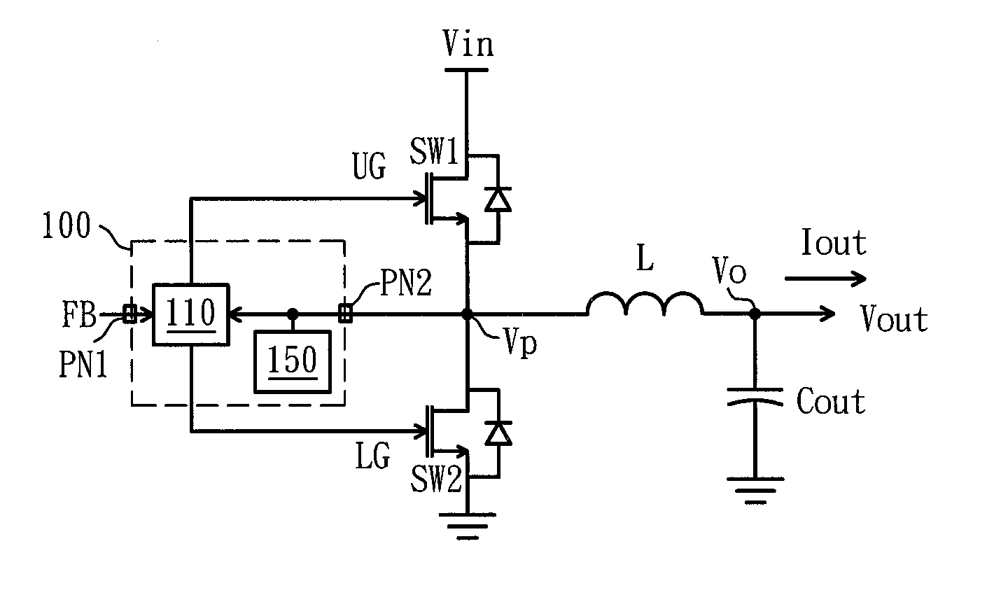
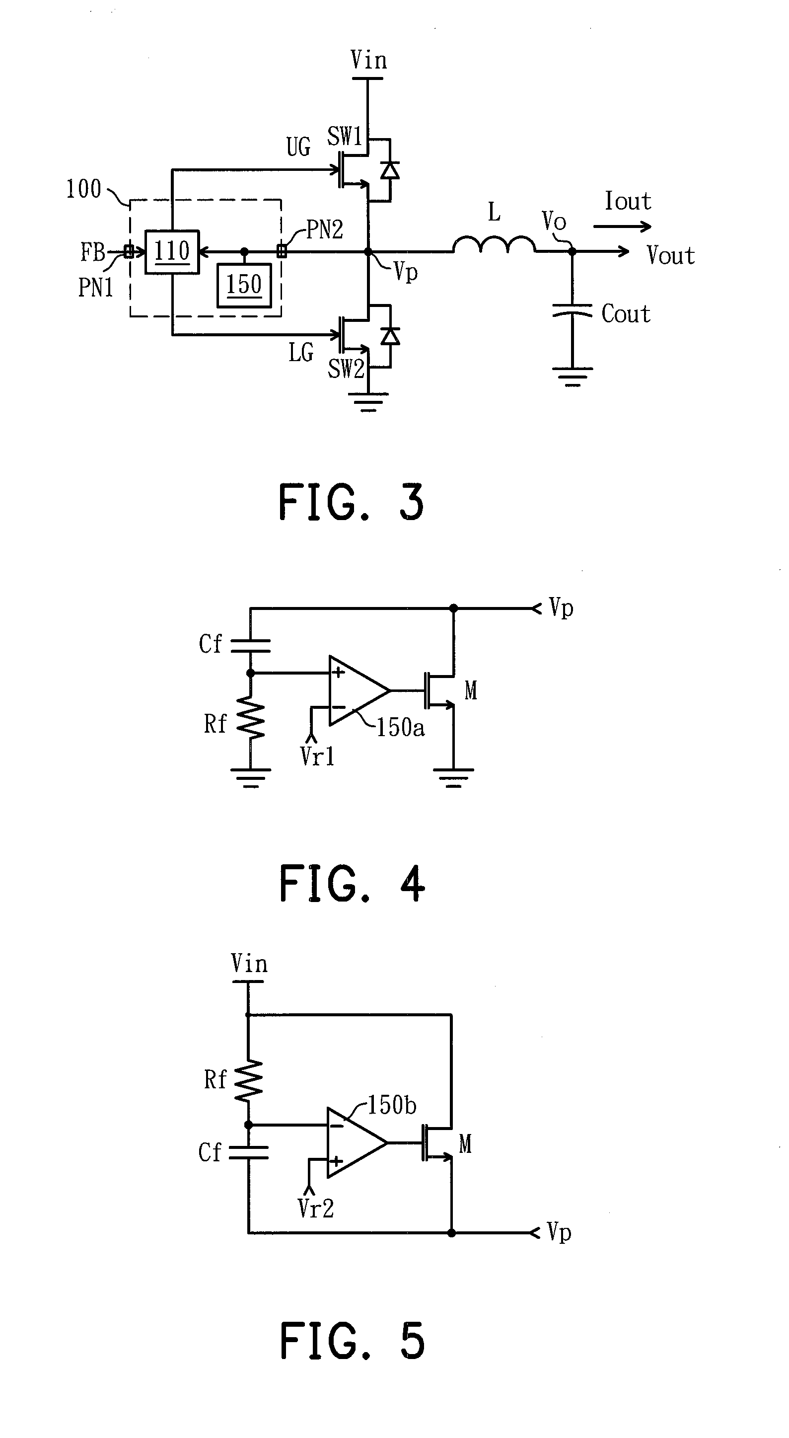
[0028]FIG. 4 is a diagram of a spike suppression circuit according to the invention. The spike suppression circuit includes an energy release path and a detection circuit. The energy release path includes a transistor M. The detection circuit includes a capacitor Cf, a resistor Rf, and a comparator 150a. One end of the resistor Rf is grounded, and the other end thereof is connected to the capacitor Cf and the non-inverting input terminal of the comparator 150a. One terminal of the transistor M is connected to another end of the capacitor Cf and the connection point as shown in FIG. 3 for receiving the voltage signal Vp on the connection point, and the other terminal of the transistor M is coupled to a reference voltage (for example, is grounded). The inverting input terminal of the comparator 150a receives a first reference voltage Vr1, and the output terminal thereof is coupled to the control terminal of the transistor M for controlling the on / off of the transistor M. When the volt...
second embodiment
[0029]FIG. 5 is a diagram of a spike suppression circuit according to the invention. The spike suppression circuit includes an energy release path and a detection circuit. The energy release path includes a transistor M. The detection circuit includes a capacitor Cf, a resistor Rf, and a comparator 150b. Unlike that in the spike suppression circuit illustrated in FIG. 4, in the present embodiment, the reference voltage is changed from the ground voltage to the input power Vin, the non-inverting input terminal of the comparator 150b receives a second reference voltage Vr2, and the inverting input terminal thereof is connected to the connection point of the capacitor Cf and the resistor Rf. When the voltage signal Vp carries a high-frequency voltage signal and accordingly the voltage on the connection point of the capacitor Cf and the resistor Rf is lower than the second reference voltage Vr2, the comparator 150b outputs a high-level signal to turn on the transistor M, so as to preven...
fourth embodiment
[0037]FIG. 11 is a diagram of a spike suppression circuit according to the invention. The spike suppression circuit in the present embodiment includes a Zener diode ZD. One end of the Zener diode ZD is coupled to a connection point on which spikes are to be suppressed, and the other end thereof is grounded, so that the peak voltage level of the voltage signal Vp is suppressed to be around the breakdown voltage of the Zener diode ZD.
[0038]In summary, high-frequency voltage oscillation may be produced by an inductive component (for example, an inductor, a transformer, a piezo transformer, a parasitic inductor, or any other component with an inductance value in a circuit) when switching units are switched, and which may shorten the lifespan of the circuit. Accordingly, the invention provides a spike suppression circuit which can reduce the amplitude of high-frequency voltage oscillation in spikes, so that the lifespan of circuits and devices can be prolonged.
PUM
 Abstract
Description
Claims
Application Information
 - R&D
- Intellectual Property
- Life Sciences
- Materials
- Tech Scout
- Unparalleled Data Quality
- Higher Quality Content
- 60% Fewer Hallucinations
Browse by: Latest US Patents, China's latest patents, Technical Efficacy Thesaurus, Application Domain, Technology Topic, Popular Technical Reports.
© 2025 PatSnap. All rights reserved.Legal|Privacy policy|Modern Slavery Act Transparency Statement|Sitemap|About US| Contact US: help@patsnap.com