Eureka AIR delivers breakthrough ideas for toughest innovation challenges, trusted by R&D personnel around the world.

Photoelectric converter

a photoelectric converter and converter technology, applied in the direction of capacitors, solid-state devices, electrolytic capacitors, etc., can solve the problems of low efficiency of photoelectric converters, low manufacturing cost of cells, and low efficiency of solar cells

Inactive Publication Date: 2012-05-24
RICOH KK
View PDF4 Cites 31 Cited by
  • Summary
  • Abstract
  • Description
  • Claims
  • Application Information

AI Technical Summary

Benefits of technology

The patent describes a photoelectric converter that includes multiple cells. Each cell has a transparent electrode and a photoelectric conversion layer with an electron transport material and a hole transport material. The cells are arranged in a porous electroconductive layer closer to the substrate. The technical effect of this design is that it allows for efficient photon absorption and electron transport, resulting in improved performance of the photoelectric converter.

Problems solved by technology

Since these solar cells have high manufacturing costs at the present time, the solar cells are not broadly used.
Specifically, when plural kinds of dyes are present on a semiconductor layer while mixed, exchange of electrons between the dyes or recombination of electrons and holes is caused, or electrons transferred from a dye to the semiconductor layer are caught by another dye, and thereby the number of electrons sent from the exited photosensitizing dye to the transparent electrode is decreased, resulting in serious decrease of the quantum yield (i.e., a ratio of generated current to absorbed photoelectrons).
However, the DSSC has a drawback in that light is absorbed by an intermediate electrode, and therefore the second layer insufficiently generates electricity.

Method used


Image

  • Photoelectric converter
  • Photoelectric converter
  • Photoelectric converter

Examples


example 1

[0236]A DSSC was prepared as follows.

[0237]Initially, a glass plate with a thickness of 1 mm, a surface of which was coated with a material SnO2:F serving as the first electrode, was provided. When the resistance between two terminals of the first electrode was measured to determine the sheet resistance thereof, the sheet resistance was about 20Ω.

[0238]Next, a nano-sized titanium oxide dispersion (SP210 from Showa Titanium Co., Ltd.) was applied on the first electrode by spin coating, followed by annealing for 15 minutes at 120° C. Thus, a titanium oxide particle layer serving as an electron transport layer was prepared.

[0239]Further, an ethanol solution of a dye D131 having the below-mentioned formula (3) was applied on the titanium oxide particle layer by spin coating, followed by annealing for 10 minutes at 120° C. Thus, a first photoelectric conversion layer including the titanium oxide particle layer and the dye D131 was prepared.

[0240]Next, a layer of ZnS—SiO2 (8 / 2 by mol) hav...

example 2

[0251]A glass plate with a thickness of 1 mm coated with SnO2:F (first electrode) was provided.

[0252]Next, a nano-sized titanium oxide dispersion (T20 from SOLARONIX SA) was applied on the first electrode by a printing method, followed by annealing for 30 minutes at 550° C. Thus, a titanium oxide particle layer with a thickness of 9 μm was prepared.

[0253]In addition, a solution SNOW LATEX MIBK-SZC from Nissan Chemical industries Ltd., which includes silica as a solid component, methyl isobutyl ketone, and methanol at a weight ratio of 45%, 50% and 5%, was applied on the above-prepared titanium oxide particle layer by spin coating at a revolution of 2500 rpm.

[0254]Further, the following components were mixed to prepare a coating liquid.

SNOW LATEX MEK-20401part(silica, from Nissan Chemical industries Ltd.)Aqueous urethane resin5parts(HW-140SF from Dainippon Ink and Chemicals Inc.)2,2,3,3-tetrafluoropropanol95parts(from Daikin Industries, Ltd.)

[0255]The coating liquid was applied on th...

example 3

[0264]A glass plate with a thickness of 1 mm coated with SnO2:F (first electrode) was provided.

[0265]A nano-sized titanium oxide dispersion was coated on the first electrode by spin coating to prepare a dense titanium oxide layer thereon.

[0266]Next, a nano-sized titanium oxide dispersion (T20 from SOLARONIX SA) was applied on the dense titanium oxide layer by a printing method, followed by annealing for 30 minutes at 550° C. Thus, a titanium oxide particle layer with a thickness of 9 μm was prepared.

[0267]In addition, a solution SNOW LATEX MIBK-SZC from Nissan Chemical industries Ltd., which includes silica as a solid component, methyl isobutyl ketone, and methanol at a weight ratio of 45%, 50% and 5%, was applied on the above-prepared titanium oxide particle layer by spin coating at a revolution of 2,500 rpm.

[0268]Further, the following components were mixed to prepare a coating liquid.

SNOW LATEX MEK-20401part(silica, from Nissan Chemical industries Ltd.)Aqueous urethane resin5part...


PUM


Abstract

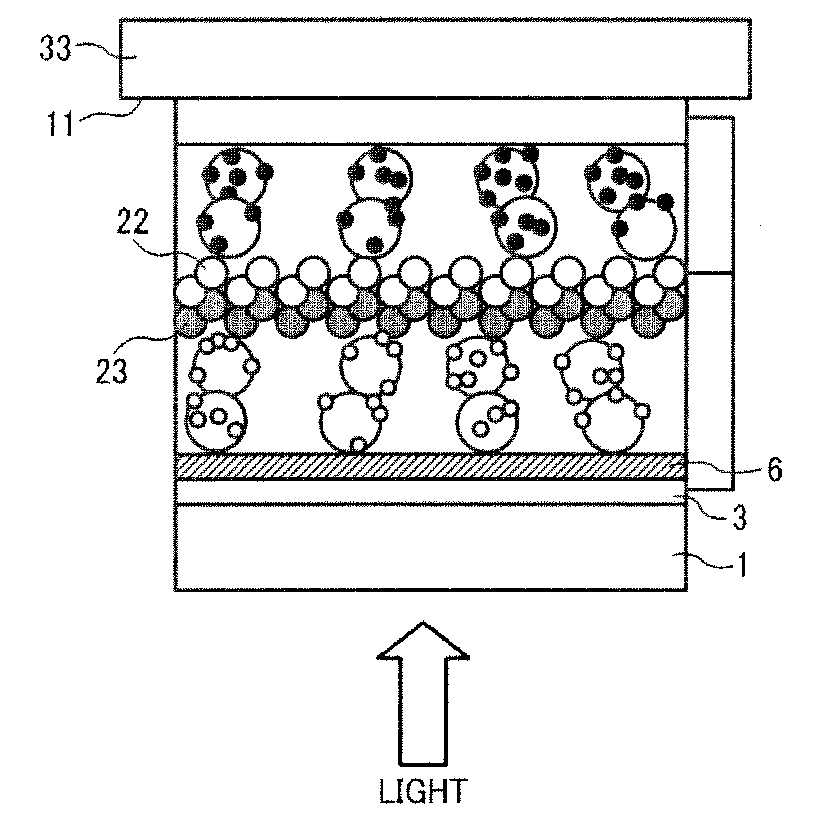
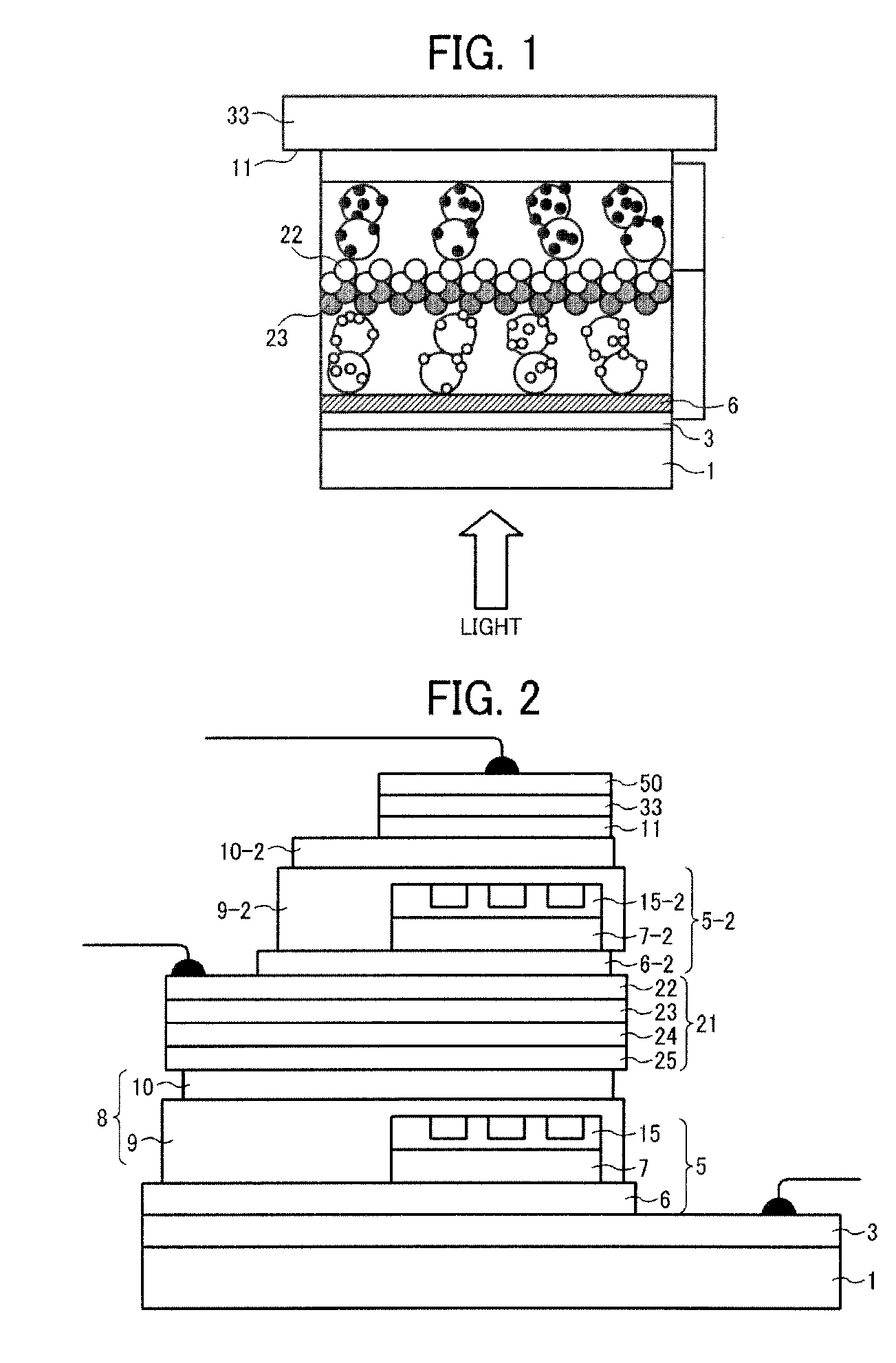
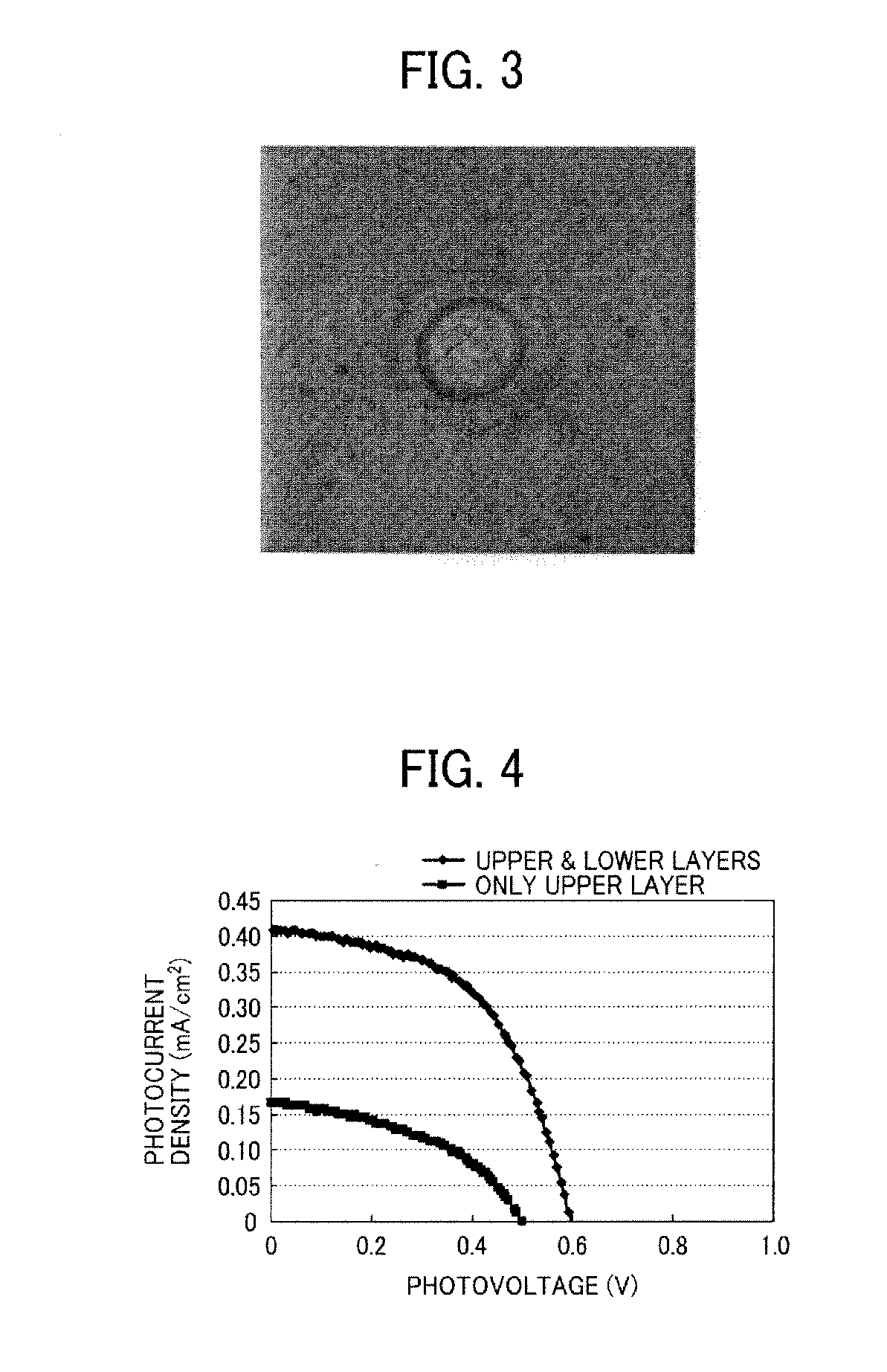
The photoelectric converter includes a substrate; and multiple cells located on the substrate so as to be overlaid. The first cell contacted with the substrate includes a transparent electrode located on the substrate, and a first photoelectric conversion layer located on the transparent electrode. The other cell or each of the others of the multiple cells includes a porous electroconductive layer located closer to the substrate and including an electroconductive material, and a photoelectric conversion layer located on the porous electroconductive layer. Each of the photoelectric conversion layers of the multiple cells includes an electron transport layer including an electron transport material, a dye connected with or adsorbed on the electron transport material, and a hole transport material. The hole transport material is also contained in voids of the porous electroconductive layer.

Description

CROSS-REFERENCE TO RELATED APPLICATIONS[0001]This patent application is based on and claims priority pursuant to 35 U.S.C. §119 to Japanese Patent Application No. 2010-261429, filed on Nov. 24, 2010, in the Japan Patent Office, the entire disclosure of which is hereby incorporated herein by reference.FIELD OF THE INVENTION[0002]This disclosure relates to a photoelectric converter. Particularly, this disclosure relates to a layered photoelectric converter, which is layered using an electrode capable of transmitting a hole.BACKGROUND OF THE INVENTION[0003]There are several types of solar cells, but almost all the commercialized solar cells are diode type solar cells in which silicone semiconductors are connected. Since these solar cells have high manufacturing costs at the present time, the solar cells are not broadly used.[0004]In attempting to reduce costs of solar cells, Mr. Graetzel of EPL Lausanne in Switzerland et al. propose a dye-sensitized solar cell with a high efficiency as...

Claims


Application Information

Patent Timeline
Patent Type & Authority Applications(United States)
IPC IPC(8): H01L51/44
CPCH01G9/2059Y02E10/542H01G9/2072
Inventor KAMEZAKI, HISAMITSUNAIJO, YOSHIHISAYASHIRO, TOHRUHORIUCHI, TAMOTSUTORII, MASAFUMI
Owner RICOH KK
Why Eureka
Eureka Blog
Learn More