Shallow trench isolation structure and method for forming the same

a technology of isolation structure and trenches, which is applied in the direction of semiconductor devices, basic electric elements, electrical appliances, etc., can solve the problems of performance degradation, high leakage current of semiconductor devices, and the influence of semiconductor devices becoming increasingly serious, so as to reduce the influence of divots on the performance of semiconductor devices, reduce the influence of mos transistor performance, and improve the effect of semiconductor devices

Active Publication Date: 2012-05-24
INST OF MICROELECTRONICS CHINESE ACAD OF SCI
View PDF13 Cites 9 Cited by
  • Summary
  • Abstract
  • Description
  • Claims
  • Application Information

AI Technical Summary

Benefits of technology

[0051]In the present invention, a first trench is firstly formed within a semiconductor substrate and is filled into the first trench to form an epitaxial layer, wherein the upper surface of the epitaxial layer is higher than that of the semiconductor substrate. Then, a second trench is formed on the epitaxial layer and filled with a first dielectric layer, wherein the width of the second trench is smaller than that of the first trench, whereby dimensions of divots formed between the first dielectric layer and the epitaxial layer are smaller, and influences of the divots on performance of the semiconductor device are reduced.
[0052]In addition, the surface of the second epitaxial layer is higher than that of the semiconductor substrate, therefore, the divots formed between the first dielectric layer and the second epitaxial layer are located above the surface of the semiconductor substrate. Meanwhile, the semiconductor device is formed on the surface of the semiconductor substrate which is between the STIs, thereby reducing the influences on performance of the MOS transistors fabricated on the semiconductor substrate.
[0053]Furthermore, the material of the epitaxial layer is different from that of the semiconductor substrate, which may cause stress on the semiconductor substrate, thereby improving performance of the semiconductor device.

Problems solved by technology

The divots 12 may lead to high leakage current and performance degradation of the semiconductor device.
Moreover, with the scaling of the dimension of semiconductor devices, the dimension of the divots relative to the semiconductor device formed between the STIs becomes bigger, influences on performance of the semiconductor device become increasingly serious.

Method used


Image

  • Shallow trench isolation structure and method for forming the same
  • Shallow trench isolation structure and method for forming the same
  • Shallow trench isolation structure and method for forming the same

Examples


Embodiment Construction

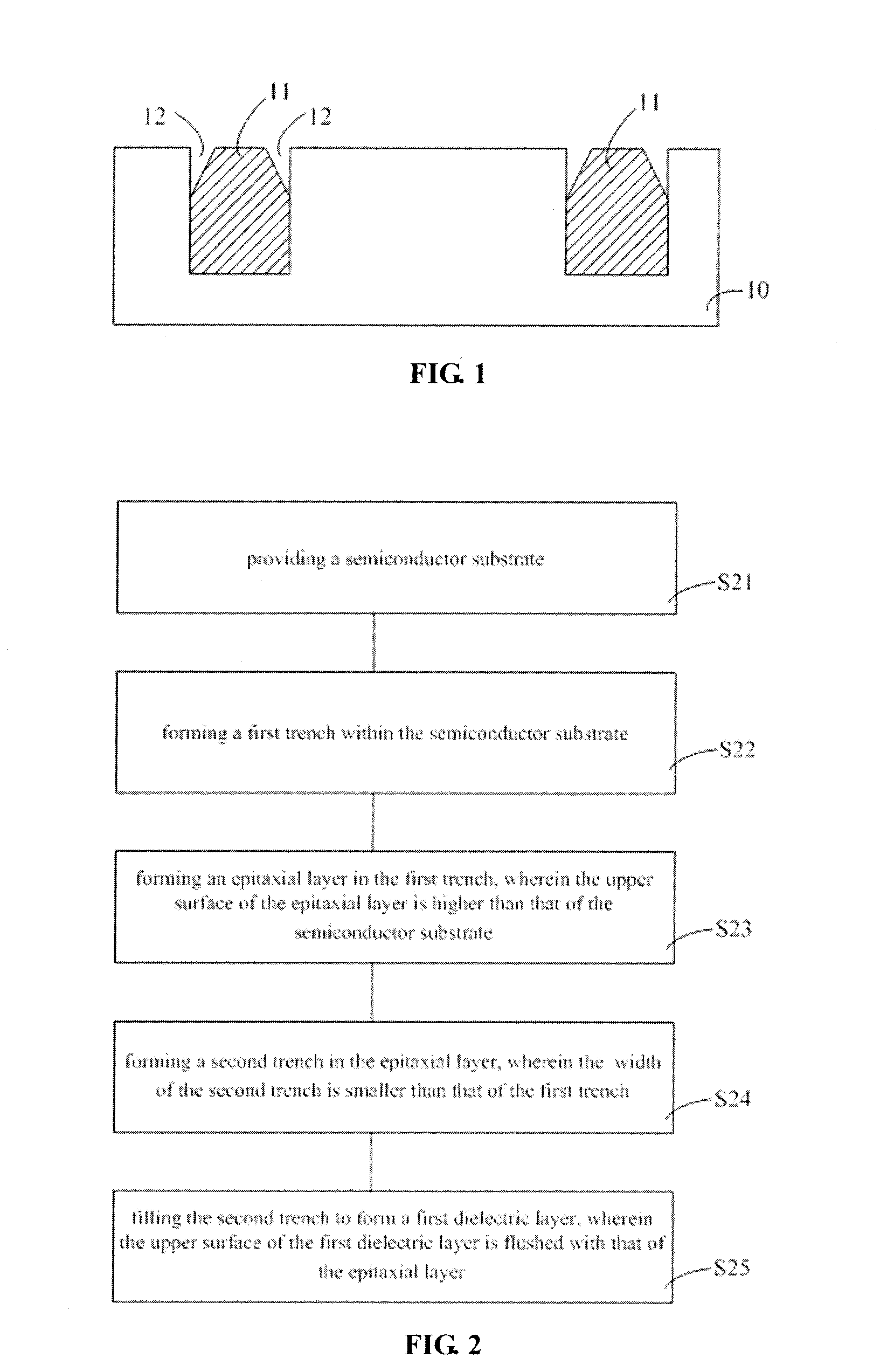
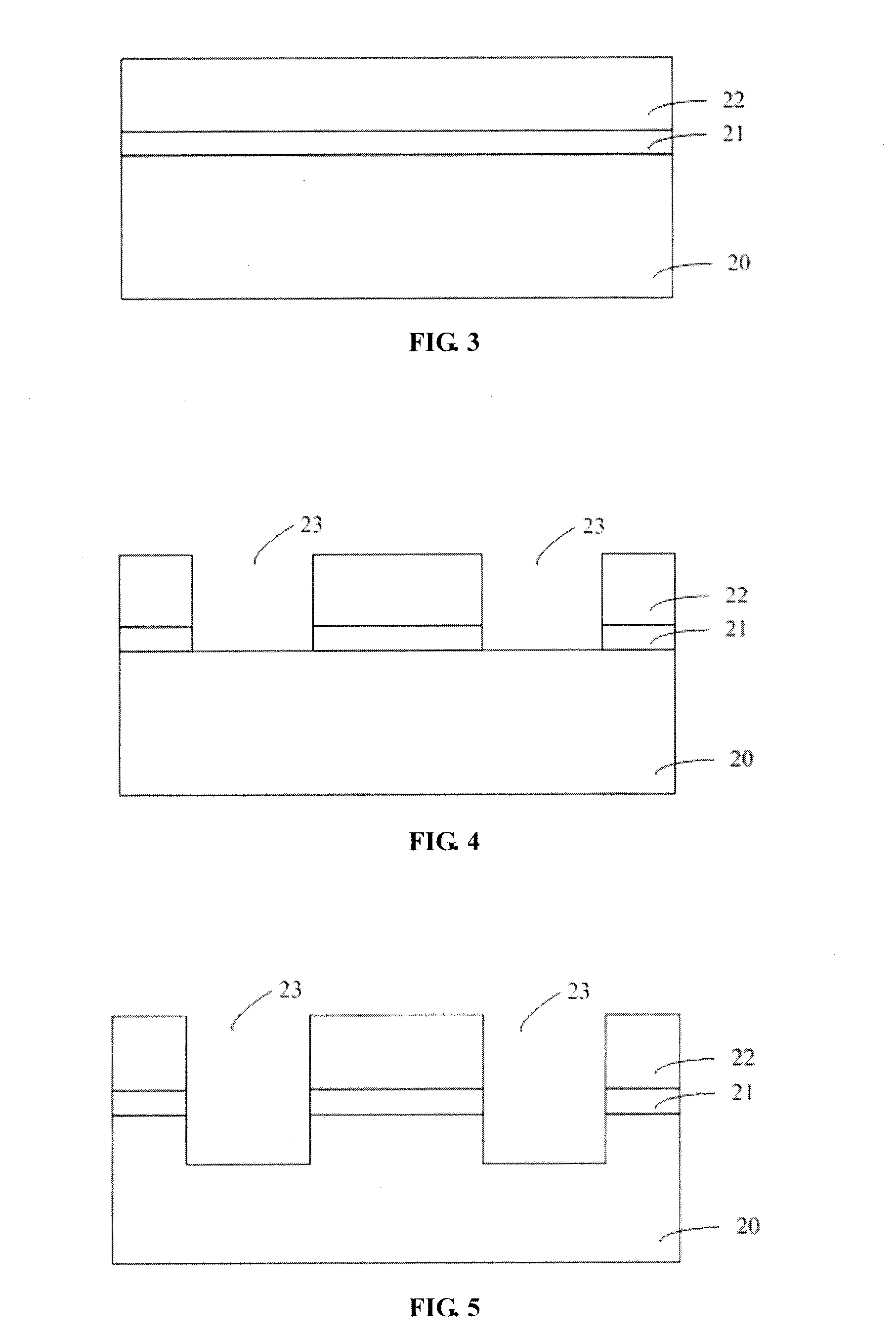
[0058]In STI structures manufactured in the prior art, divots are formed between a surface of the dielectric material filled in the STIs and a surface of the substrate, which may lead to leakage current and performance degradation of the semiconductor device.

[0059]According to the present invention, firstly, a first trench is formed in a semiconductor substrate, and the first trench is filled to form an epitaxial layer. Then, a second trench is formed in the epitaxial layer, and the second trench is filled to form a first dielectric layer. The surface of the epitaxial layer is higher than that of the semiconductor substrate, and the width of the second trench is smaller than that of the first trench. Because the width of the second trench is smaller than that of the first trench, the dimension of the divots formed between the first dielectric material and the epitaxial layer is small, which is advantageous to alleviate negative effects of the divots on performance of the semiconduct...


PUM


Abstract

The invention provides a STI structure and a method for manufacturing the same. The STI includes a semiconductor substrate; a first trench formed on the upper surface of the semiconductor substrate and filled with an epitaxial layer, wherein the upper surface of the epitaxial layer is higher than that of the semiconductor substrate; and a second trench formed on the epitaxial layer and filled with a first dielectric layer, wherein the upper surface of the first dielectric layer is flush with that of the epitaxial layer, and the width of the second trench is smaller than that of the first trench. The invention reduces the influences of divots on performance of the semiconductor device.

Description

CROSS REFERENCE TO RELATED APPLICATIONS[0001]The present application claims priority to PCT Application No. PCT / CN2011 / 070693, filed Jan. 27, 2011, which claimed priority to Chinese Patent Application No. 201010552589.8, entitled “SHALLOW TRENCH ISOLATION STRUCTURE AND METHOD FOR FORMING THE SAME”, filed Nov. 19, 2010. Both the PCT application and the Chinese application are incorporated herein by reference in their entireties.FIELD OF THE INVENTION[0002]The present invention relates to semiconductor manufacturing technology, and particularly, relates to a Shallow Trench Isolation (STI) structure and a method for manufacturing the same.BACKGROUND OF THE INVENTION[0003]As the semiconductor technology advances into deep submicron era, active areas of semiconductor devices, such as a MOS transistor, are generally isolated by STI structures. The method for fabricating the shallow trench isolation structure comprises: forming a shallow trench on a substrate by an etching process for isol...

Claims


Application Information

Patent Timeline
Patent Type & Authority Applications(United States)
IPC IPC(8): H01L29/12H01L29/16H01L21/761H01L27/04H01L21/762
CPCH01L29/7846H01L21/76224
Inventor ZHONG, HUICAIYIN, HAIZHOULIANG, QINGQINGZHU, HUILONG
Owner INST OF MICROELECTRONICS CHINESE ACAD OF SCI
Why Eureka
Try Eureka