Light-Emitting Element, Manufacturing Method Thereof, and Lighting Device

a technology of light-emitting elements and manufacturing methods, which is applied in the field of light-emitting elements, can solve the problems of reducing difficult to fill defect portions in the electroluminescent layer with insulating materials, and easy deterioration of the electroluminescent layer, so as to prevent short circuit between the first electrode and the second electrode, the effect of suppressing the emission characteristics of light-emitting elements

Inactive Publication Date: 2012-05-24
SEMICON ENERGY LAB CO LTD
View PDF1 Cites 21 Cited by
  • Summary
  • Abstract
  • Description
  • Claims
  • Application Information

AI Technical Summary

Benefits of technology

[0011]Moreover, the conventional technique of preventing a short circuit between the first electrode and the second electrode has a problem in that the electroluminescent layer easily deteriorates when the defect portion in the electroluminescent layer is filled with the insulating material, which causes a reduction in the emission characteristics of the light-emitting element. For example, in the case where the electroluminescent layer is formed using an organic compound, the electroluminescent layer is melted or peeled when the defect portion in the electroluminescent layer is filled with the insulating material, which causes a reduction in the emission characteristics of the light-emitting element.
[0012]An object of one embodiment of the present invention is to suppress a reduction in the emission characteristics of a light-emitting element while preventing a short circuit between a first electrode and a second electrode of the light-emitting element.
[0014]The structure makes it possible to prevent the formation of the insulating material on a portion other than the defect portion in the electroluminescent layer, to suppress a reduction in the emission characteristics of the light-emitting element, while preventing a short circuit between the first electrode and the second electrode.
[0016]The structure enables the metal oxide layer to function as a protective layer so that the deterioration of the light-emitting element at the time when the defect portion in the electroluminescent layer is filled with the insulating material is reduced.
[0017]One embodiment of the present invention includes the steps of forming a conductive layer functioning as a first electrode; forming an electroluminescent layer over the conductive layer functioning as a first electrode; filling a defect portion existed in the electroluminescent layer with an insulating material so that the defect portion is sealed; and forming a conductive layer functioning as a second electrode over the electroluminescent layer and the insulating material so that the conductive layer functioning as a second electrode overlaps with the conductive layer functioning as a first electrode with the electroluminescent layer and the insulating material interposed therebetween. In the method, an insulating layer may be formed over the electroluminescent layer and the insulating layer may be selectively removed so that only part of the insulating layer, which fills the defect portion in the electroluminescent layer, remains. A light-emitting element is manufactured by the method, whereby a reduction in the emission characteristics of the light-emitting element can be suppressed and a short circuit between the first electrode and the second electrode can be prevented.
[0019]According to one embodiment of the present invention, the formation of the insulating material between the electroluminescent layer and the second electrode can be suppressed as much as possible; thus, a reduction in the emission characteristics of the light-emitting element can be suppressed and a short circuit between the first electrode and the second electrode can be prevented.

Problems solved by technology

However, in the conventional technique of preventing a short circuit between a first electrode and a second electrode, such as the technique described in Patent Document 1, it is difficult to fill a defect portion in the electroluminescent layer with an insulating material while preventing the insulating material from being formed on a portion other than the defect portion.
Moreover, the conventional technique of preventing a short circuit between the first electrode and the second electrode has a problem in that the electroluminescent layer easily deteriorates when the defect portion in the electroluminescent layer is filled with the insulating material, which causes a reduction in the emission characteristics of the light-emitting element.

Method used


Image

  • Light-Emitting Element, Manufacturing Method Thereof, and Lighting Device
  • Light-Emitting Element, Manufacturing Method Thereof, and Lighting Device
  • Light-Emitting Element, Manufacturing Method Thereof, and Lighting Device

Examples


embodiment 1

[0029]In this embodiment, examples of light-emitting elements will be described.

[0030]Note that the light-emitting element includes a first electrode, a second electrode, and an electroluminescent layer overlapping with the first electrode and the second electrode and emits light emitted from the electroluminescent layer in accordance with voltage applied between the first electrode and the second electrode.

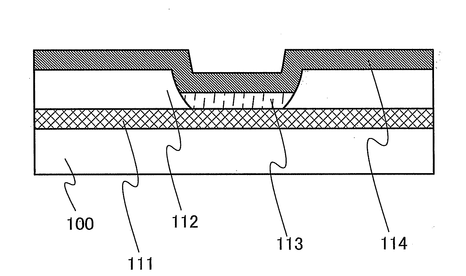
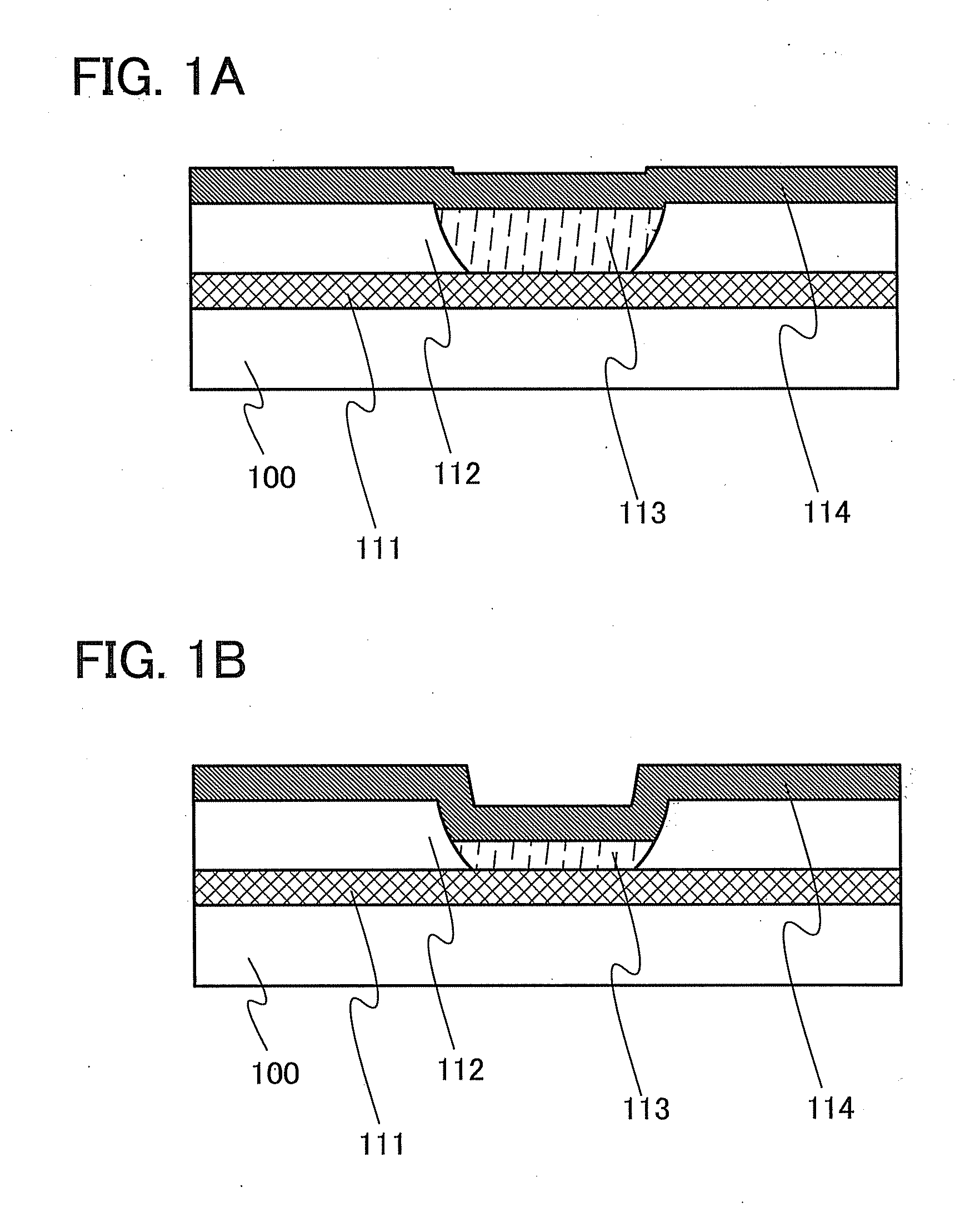
[0031]Structural examples of light-emitting elements in this embodiment will be described with reference to FIGS. 1A and 1B. FIGS. 1A and 1B are cross-sectional schematic views illustrating the structural examples of the light-emitting elements in this embodiment.

[0032]The light-emitting elements illustrated in FIGS. 1A and 1B each include a conductive layer 111, an electroluminescent layer 112, an insulating material 113, and a conductive layer 114.

[0033]The conductive layer 111 is formed over, for example, a layer 100 over which an element is formed (hereinafter, an element for...

embodiment 2

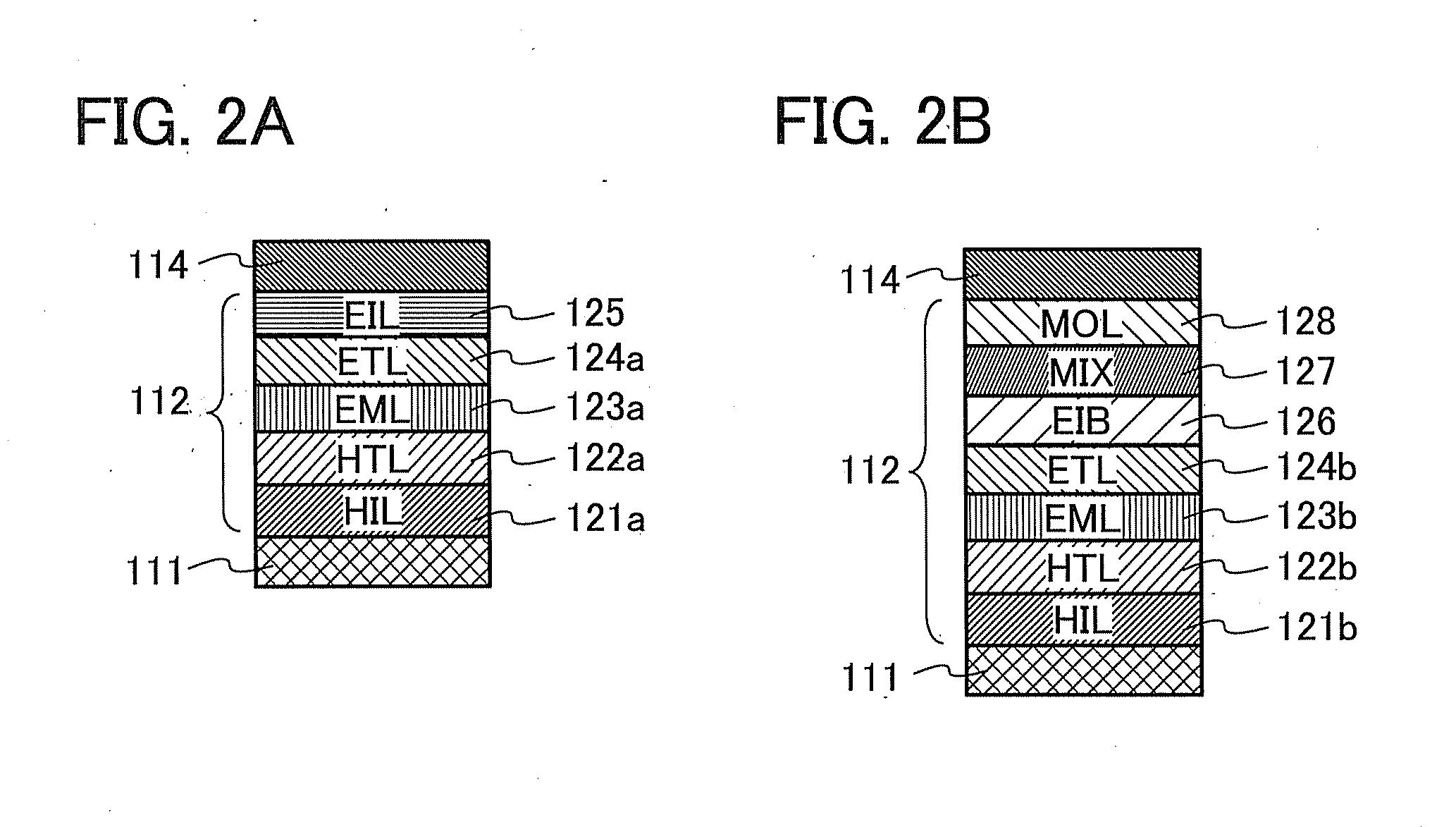
[0053]In this embodiment, structural examples of the electroluminescent layer of the light-emitting element in Embodiment 1 will be described.

[0054]Structural examples of the electroluminescent layer 112 illustrated in FIG. 1A will be described with reference to FIGS. 2A and 2B as a structural example of the electroluminescent in this embodiment. FIGS. 2A and 2B are each a schematic view illustrating the structural example of the electroluminescent layer in this embodiment.

[0055]The electroluminescent layer 112 illustrated in FIG. 2A includes a hole-injection layer (HIL) 121a, a hole-transport layer (HTL) 122a, a light-emitting layer (EML) 123a, an electron-transport layer (ETL) 124a, and an electron-injection layer (EIL) 125.

[0056]The hole-injection layer 121a is provided over the conductive layer 111 illustrated in FIG. 1A. Note that the hole-injection layer 121a is not necessarily provided.

[0057]The hole-transport layer 122a is provided over the hole-injection layer 121a. Note th...

embodiment 3

[0138]In this embodiment, an example of a manufacturing method of the light-emitting element described in Embodiment 1 will be described.

[0139]As an example of a manufacturing method of a light-emitting element in this embodiment, a manufacturing method of the light-emitting element illustrated in FIG. 1A will be described with reference to FIGS. 3A to 3E. FIGS. 3A to 3E are cross-sectional schematic views illustrating the example of the manufacturing method of the light-emitting element illustrated in FIG. 1A.

[0140]First, as illustrated in FIG. 3A, the conductive layer 111 is formed over the element formation layer 100.

[0141]The conductive layer 111 can be formed by, for example, forming a film of a material applicable to the conductive layer 111 over the element formation layer 100 by a sputtering method. The conductive layer 111 may also be formed by stacking films of materials applicable to the conductive layer 111.

[0142]Next, as illustrated in FIG. 3B, the electroluminescent la...


PUM


Abstract

A light-emitting element includes a conductive layer functioning as a first electrode, an electroluminescent layer, and a conductive layer functioning as a second electrode, and further includes an insulating material filling a defect portion in the electroluminescent layer so that the defect portion is sealed. In the light-emitting element, the conductive layer functioning as a second electrode overlaps with the conductive layer functioning as a first electrode with the electroluminescent layer and the insulating material interposed therebetween and is in contact with a top surface of the electroluminescent layer.

Description

BACKGROUND OF THE INVENTION[0001]1. Field of the Invention[0002]One embodiment of the present invention relates to a light-emitting element. One embodiment of the present invention relates to a lighting device including the light-emitting element in a light-emitting portion.[0003]2. Description of the Related Art[0004]In recent years, a light-emitting element which is one of the electro-optical elements and contains an organic compound or an inorganic compound which emits light by voltage application (the light-emitting element is also referred to as an electroluminescent element) has been developed.[0005]The light-emitting element includes at least a first electrode, a second electrode, and an electroluminescent layer overlapping with the first electrode and the second electrode and emits light in accordance with voltage applied between the first electrode and the second electrode.[0006]For example, the light-emitting element can be manufactured in such a manner that a first electr...

Claims


Application Information

Patent Timeline
Patent Type & Authority Applications(United States)
IPC IPC(8): H01L33/02H01L33/40
CPCH01L51/50H01L2251/568H01L2251/5392H01L2251/5361H10K50/00H10K2102/341H10K71/861
Inventor TANAKA, KOICHIROIKEDA, HISAOYAMAZAKI, SHUNPEI
Owner SEMICON ENERGY LAB CO LTD
Why Eureka
Try Eureka