Active matrix substrate, display device, and organic el display device
- Summary
- Abstract
- Description
- Claims
- Application Information
AI Technical Summary
Benefits of technology
Problems solved by technology
Method used
Image


Examples
embodiment 1
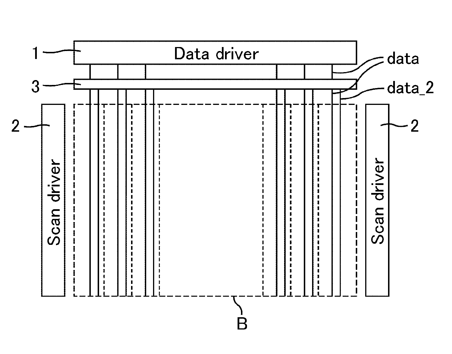
[0077]FIG. 1 shows a circuit diagram of a pixel of an organic EL display device of embodiment 1. As shown in FIG. 1, a pixel of an organic EL display device of the present embodiment includes a transistor T7 as an adjusting transistor for adjusting the voltage of a pixel electrode of an organic EL element OLED. The transistor T7 is electrically connected to a path used for supplying electric current to the organic EL element OLED from the transistor T4 (drive transistor). More specifically, the drain electrode of the transistor T7 is electrically connected to the path for supplying electric current to the organic EL element OLED from the transistor T4. The source electrode of the transistor T7 is electrically connected to a signal line “data_2”. A voltage adjusting line adj [n] is electrically connected to the gate electrode of the transistor T7. At the path for supplying electric current to the organic EL element OLED from the transistor T4, a transistor T6 for switching of the ele...
embodiment 2
[0088]FIG. 5 shows a circuit diagram of a pixel of an organic EL display device of embodiment 2. As shown in FIG. 5, the organic EL display device of embodiment 2 includes no signal line “data_2”. A source electrode of a transistor T7 is electrically connected to a signal line data. That is, the organic EL display device of embodiment 2 has the same structure as that of embodiment 1 except that the signal line to which the source electrode of the transistor T7 (adjusting transistor) is electrically connected is the same as the signal line to which the source electrode of the transistor T4 (drive transistor) is electrically connected.
[0089]In the organic EL display device of the present embodiment, the signal line to which the source electrode of the transistor T7 is electrically connected is the same as the signal line to which the source electrode of the transistor T4 is electrically connected. Therefore, the voltage of the pixel electrode adjusted by the transistor T7 is the same ...
embodiment 3
[0090]FIG. 6 shows a circuit diagram of a pixel of an organic EL display device of embodiment 3. As shown in FIG. 6, the organic EL display device of embodiment 3 has the same structure as that of embodiment 1 except that no signal line “data_2” is provided and the source electrode and a drain electrode of the transistor T7 are connected in parallel to the organic EL element OLED.
[0091]In the organic EL display device of the present embodiment, the source electrode and the drain electrode of the transistor T7 are connected in parallel to the organic EL element OLED. Therefore, the voltages of the anode and cathode of the organic EL element OLED may be the same as each other. This enables discharge of charge, which is stored in the Cad, through a power supply line ELVSS using the transistor T7 as a path for electric current. As a result, display characteristics without occurrence of the stepwise response characteristics can be achieved. The feeding of signals into respective wirings ...
PUM
 Abstract
Description
Claims
Application Information