Power-gated retention flops
- Summary
- Abstract
- Description
- Claims
- Application Information
AI Technical Summary
Problems solved by technology
Method used
Image

Examples
Embodiment Construction
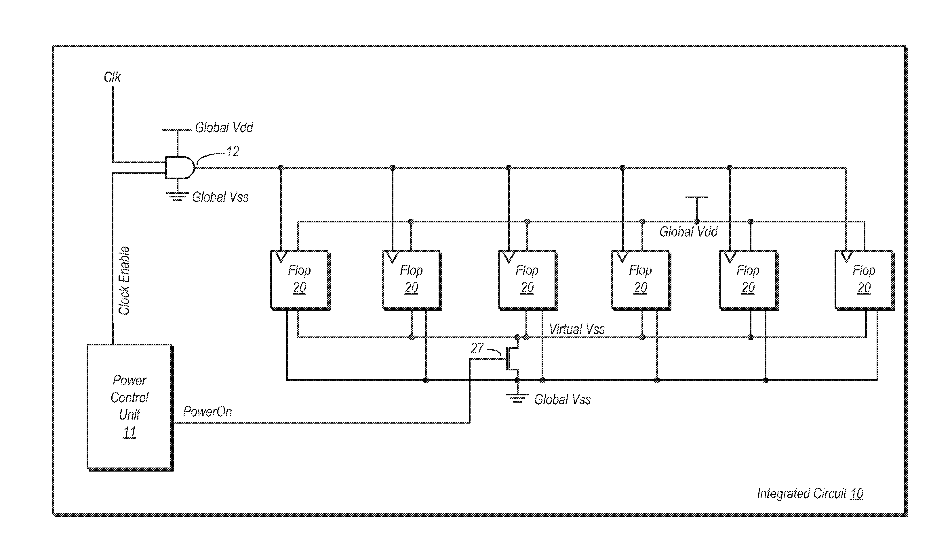
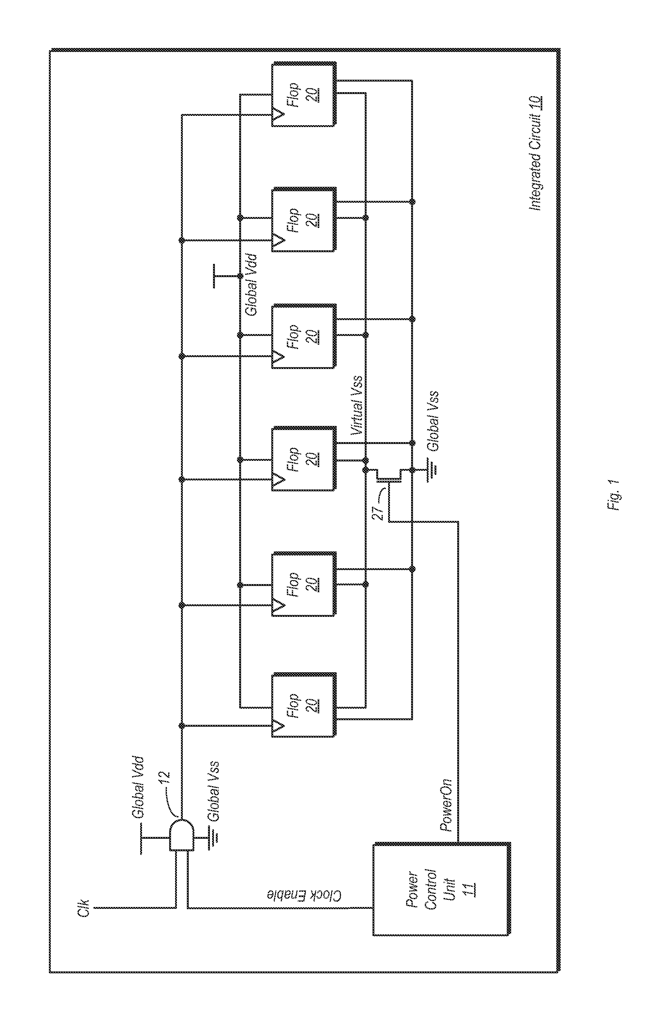
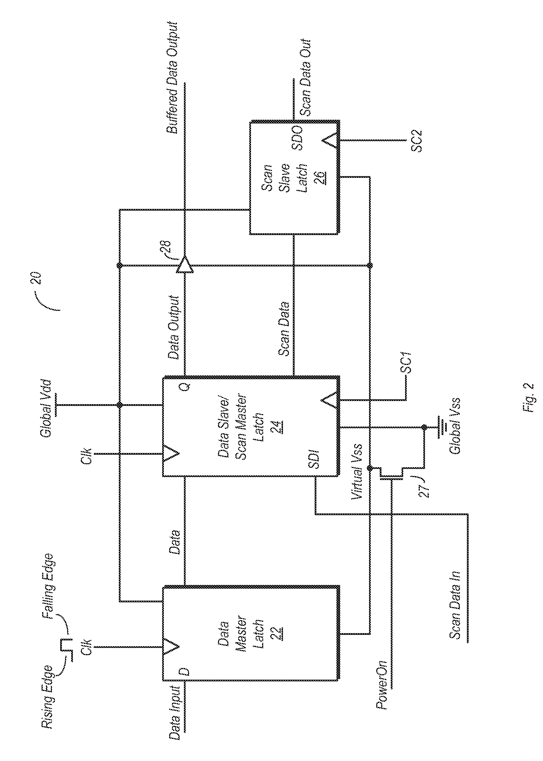
[0007]A power-gated retention flop circuit is disclosed. In one embodiment, a retention flop includes a first latch circuit coupled to a first global voltage node and a virtual voltage node and configured to receive a data input signal. The retention flop further includes a second latch circuit coupled to receive the data input signal from the first latch circuit, wherein the second latch circuit is coupled to the first global voltage node and a second global voltage node, and wherein the second latch circuit is configured to provide a data output signal based on a state of the data input signal. A power-gating circuit may be coupled between the virtual voltage node and the second global voltage node, wherein the power-gating circuit is configured to, when active, couple the virtual voltage node to the second global voltage node.
[0008]In one embodiment, a method includes providing a data signal to a data input of a first latch of a storage circuit, the storage circuit including the ...
PUM
 Abstract
Description
Claims
Application Information