Semiconductor device

a semiconductor device and semiconductor technology, applied in the direction of solid-state devices, transistors, instruments, etc., can solve the problem of overhead consumption of extra power, and achieve the effects of reducing power consumption of semiconductor devices, high speed, and cutting power consumption

Inactive Publication Date: 2013-09-12
SEMICON ENERGY LAB CO LTD
View PDF15 Cites 27 Cited by
  • Summary
  • Abstract
  • Description
  • Claims
  • Application Information

AI Technical Summary

Benefits of technology

[0032]According to one embodiment of the present invention, temperature sensors are provided in circuit blocks in a semiconductor device, temperatures of the circuit blocks are detected by the respective temperature sensors, and an off period (period during which supply of power is stopped) appropriate to each circuit block can be set. Thus, even in the case where supply of power cannot be stopped by the power gating according to the flow chart shown in FIG. 15...

Problems solved by technology

Specifically, in writing and reading processes of th...

Method used


Image

  • Semiconductor device
  • Semiconductor device
  • Semiconductor device

Examples


embodiment 1

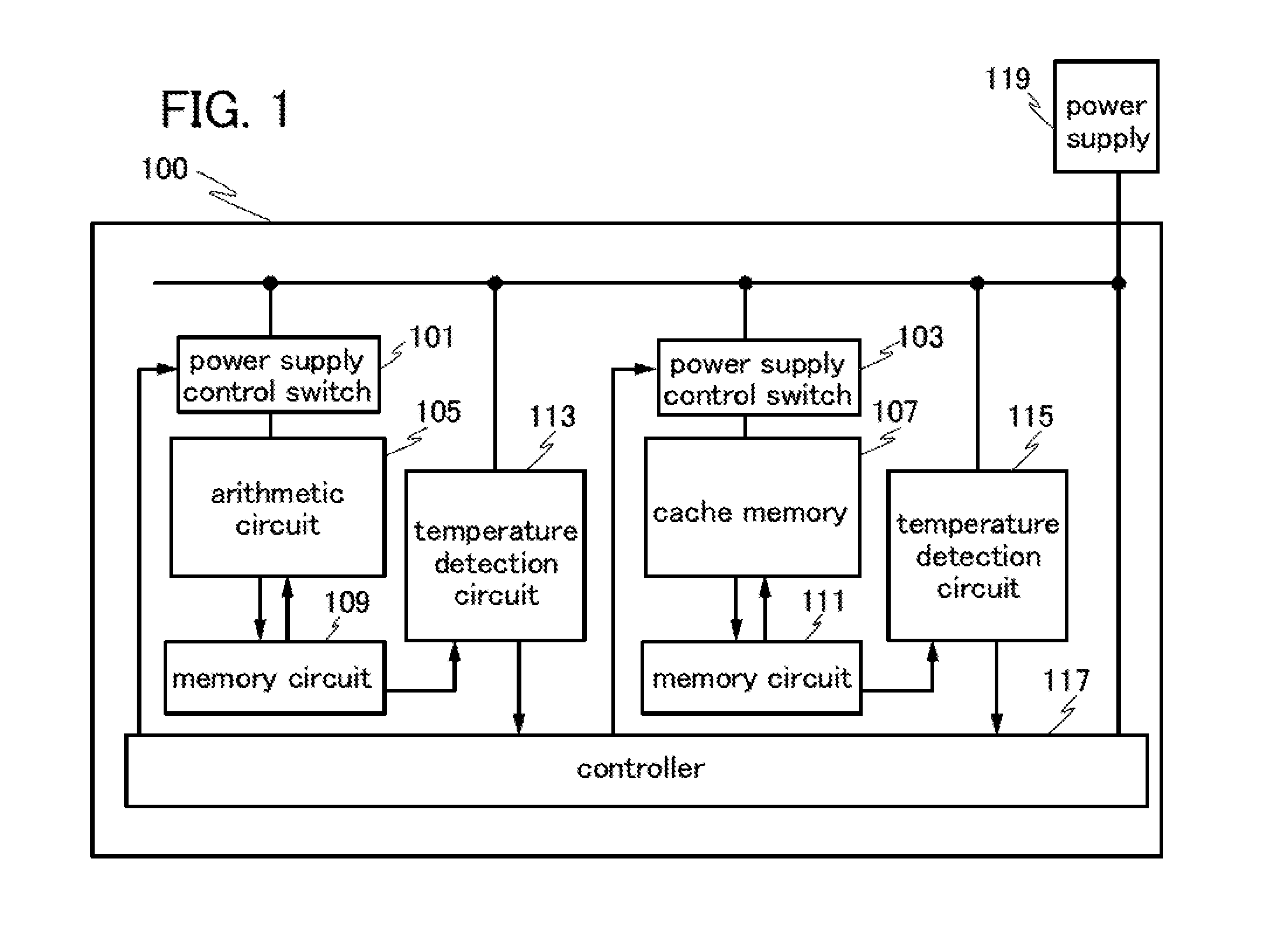
[0053]First, a structure example of a semiconductor device which is one embodiment of the present invention will be described with reference to FIG. 1. Note that in this embodiment, a processor is described as an example of a semiconductor device which is one embodiment of the present invention.

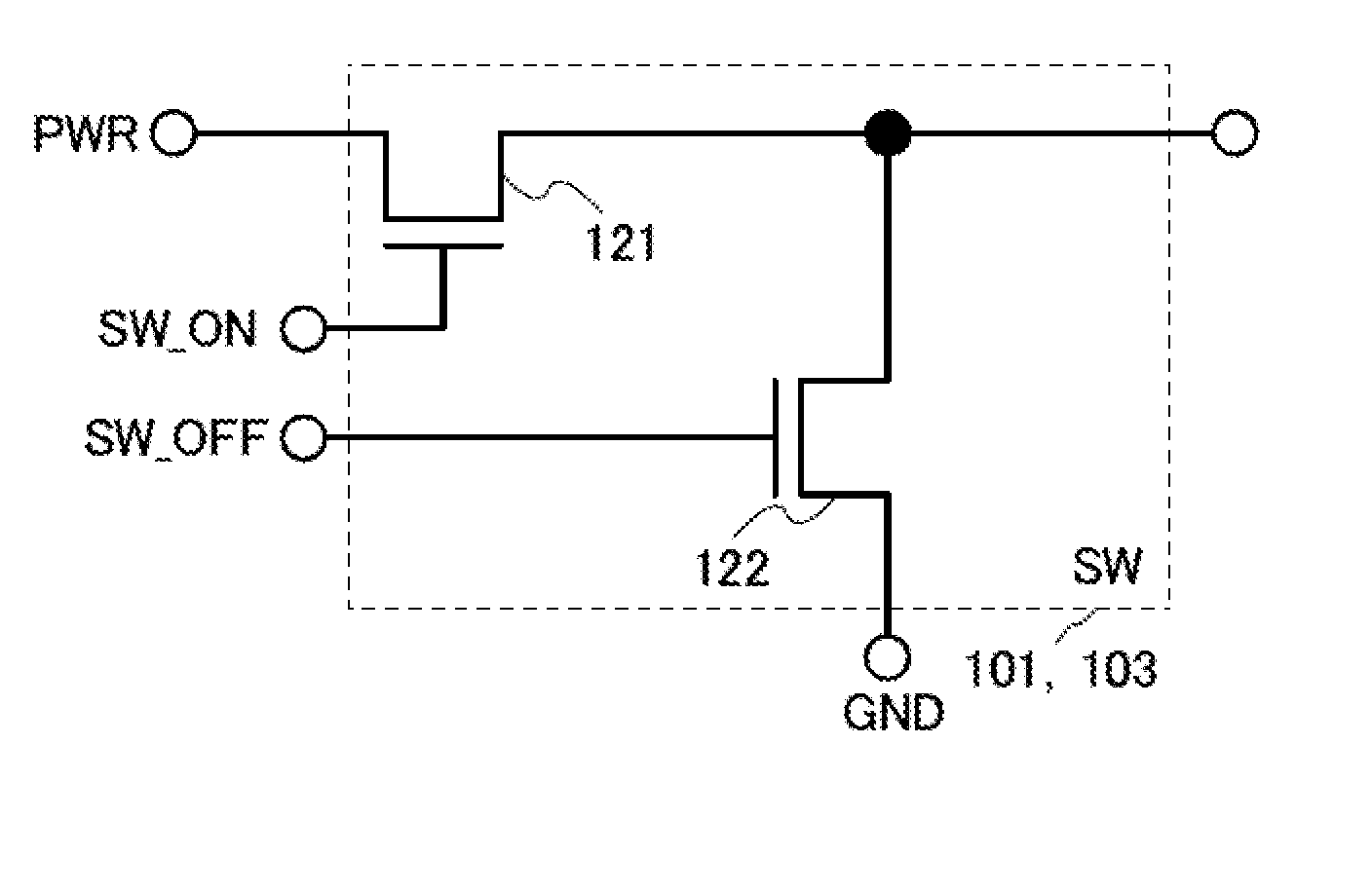
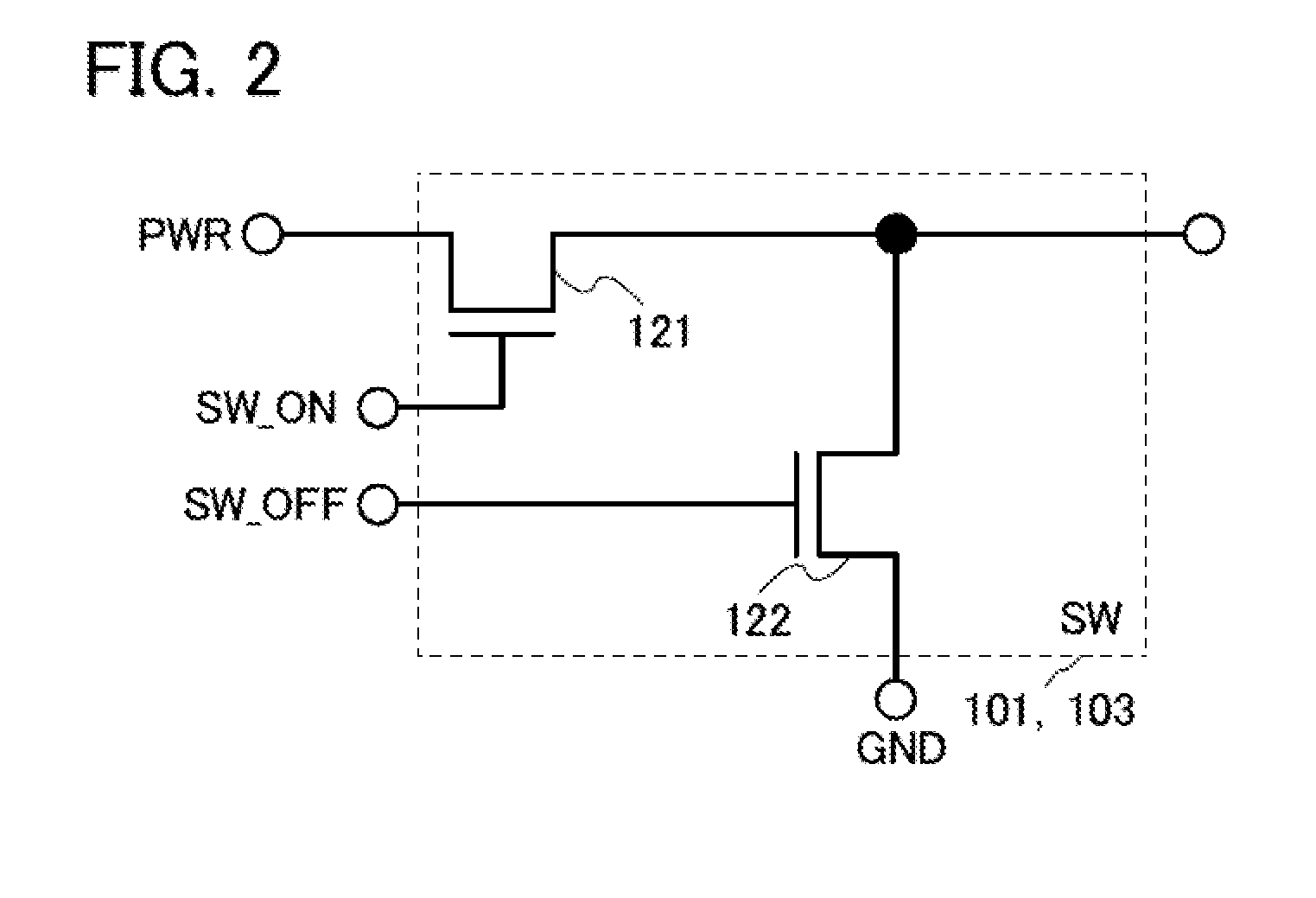
[0054]FIG. 1 is a block diagram of a processor 100. The processor 100 includes an arithmetic circuit 105 and a cache memory 107. The processor 100 includes a power supply control switch 101 functioning as a power gate between a power supply 119 and the arithmetic circuit 105 and a power supply control switch 103 functioning as a power gate between the power supply 119 and the cache memory 107. The processor 100 includes a controller 117 which controls the power supply control switch 101 and the power supply control switch 103. The processor 100 includes a memory circuit 109 which holds data obtained by the arithmetic circuit 105 and a memory circuit 111 which holds data stored in the cache me...

embodiment 2

[0125]In this embodiment, structure examples of transistors applicable to a semiconductor device which is one embodiment of the present invention will be described with reference to schematic cross-sectional views in FIGS. 11A to 11C.

[0126]Note that components illustrated in FIGS. 11A to 11C are not to scale in some cases.

[0127]The transistor illustrated in FIG. 11A includes a semiconductor layer 711, an insulating layer 714, a conductive layer 715, insulating layers 716a and 716b, an insulating layer 717, conductive layers 718a and 718b, and an insulating layer 719.

[0128]The semiconductor layer 711 is positioned over an element formation layer 700 with the insulating layer 701 interposed therebetween. Note that the semiconductor layer 711 is not necessarily provided over the insulating layer 701 and may be provided directly on the element formation layer 700.

[0129]The semiconductor layer 711 includes regions 709a and 709b which are separated from each other and to which dopant is a...

embodiment 3

[0202]In this embodiment, examples of an electronic device provided with the semiconductor device which is one embodiment of the present invention will be described with reference to drawings. In addition to the processor described in the above embodiment, a register, a register controller, an instruction decoder, an interrupt controller, a timing controller, a bus interface, and the like are provided, whereby a semiconductor device including a CPU or DSP can be formed.

[0203]Further, since the processor described in the above embodiment has superiority in cutting power consumption, in a semiconductor device including the processor, power consumption can be much lowered. FIGS. 14A to 14F illustrates specific examples of an electronic device including the semiconductor device;

[0204]The electronic device illustrated in FIG. 14A is an example of a personal digital assistant.

[0205]The electronic device illustrated in FIG. 14A includes a housing 1011 and a panel 1012, a button 1013, and a...


PUM


Abstract

To provide a semiconductor device including a plurality of circuit blocks each of which is capable of performing power gating by setting off periods appropriate to temperatures of the respective circuit blocks. Specifically, the semiconductor device includes an arithmetic circuit, a memory circuit configured to hold data obtained by the arithmetic circuit, a power supply control switch configured to control supply of the power supply voltage to the arithmetic circuit, a temperature detection circuit configured to detect the temperature of the memory circuit and to estimate overhead from the temperature, and a controller configured to set a period during which supply of the power supply voltage is stopped in the case where a power consumption of the arithmetic circuit during the period is larger than the overhead period and to control the power supply control switch.

Description

BACKGROUND OF THE INVENTION[0001]1. Field of the Invention[0002]The present invention relates to a semiconductor device.[0003]Note that a semiconductor device in this specification refers to general devices which can function by utilizing semiconductor characteristics; for example, a semiconductor integrated circuit including a semiconductor element such as a transistor, an electro-optical device such as a display device, and an electronic device are all semiconductor devices.[0004]2. Description of the Related Art[0005]The scale of semiconductor integrated circuits including logic circuits has increased year by year. Integrated circuits were constituted by several elements at an early stage of development; nowadays, there are central processing units (CPUs) and digital signal processors (DSPs) constituted by tens of millions of elements.[0006]Although power consumption per element is reduced by miniaturization and reduction in driving voltage of elements included in such CPUs and D...

Claims


Application Information

Patent Timeline
IPC IPC(8): G11C5/14
CPCG11C5/14G06F1/3203G06F1/206G11C5/148G11C7/00H01L27/1203H01L29/786
Inventor KOYAMA, JUN
Owner SEMICON ENERGY LAB CO LTD
Why Eureka
Try Eureka