Strained silicon structure

Active Publication Date: 2012-05-31
MARLIN SEMICON LTD
View PDF3 Cites 12 Cited by
  • Summary
  • Abstract
  • Description
  • Claims
  • Application Information

AI Technical Summary

Benefits of technology

[0006]Therefore, it is one objective of the present invention to provide a strained silicon structure which can control the channel strain within the high density region and the low density region.
[0009]Because the first source / drain to gate distance is smaller than the second source / drain to gate distance, the channel strain in the high density region will be higher than the channel strain in the low density region. Therefore, the entire performance of the strained silicon structure will be improved.

Problems solved by technology

Recently, however, it has appeared that the miniaturization attained by lithographic technology has reached its limit, and that carrier mobility has almost reached theoretical mobility in Si.
As a result, the strained Si channels in the high density region and the low density region may become different and deteriorate the performance of the entire device.

Method used


Image

  • Strained silicon structure
  • Strained silicon structure
  • Strained silicon structure

Examples


first embodiment

[0015]FIG. 1 to FIG. 5 are schematic cross-sectional diagrams illustrating a method of manufacturing a strained silicon structure in accordance with the present invention.

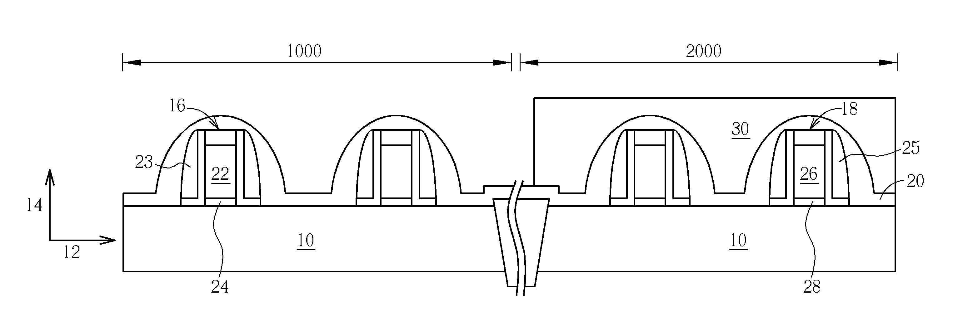
[0016]As shown in FIG. 1, a substrate 10 having a top surface is provided. The substrate 10 is defined into a low density region 1000 and a high density region 2000. The substrate 10 may be silicon substrate. A horizontal direction 12 is parallel to the top substrate of the substrate 10. A vertical direction 14 is perpendicular to the top surface of the substrate 10. Numerous first gate structures 16 are disposed within the low density region 1000, and numerous second gate structures 18 are disposed within the high density region 2000. The shortest distance between each first gate structure 16 is shorter than the shortest distance between each second gate structure 18. The first gate structure 16 includes a first gate 22 and a first gate dielectric layer 24. The first gate dielectric layer 24 is disposed between th...

second embodiment

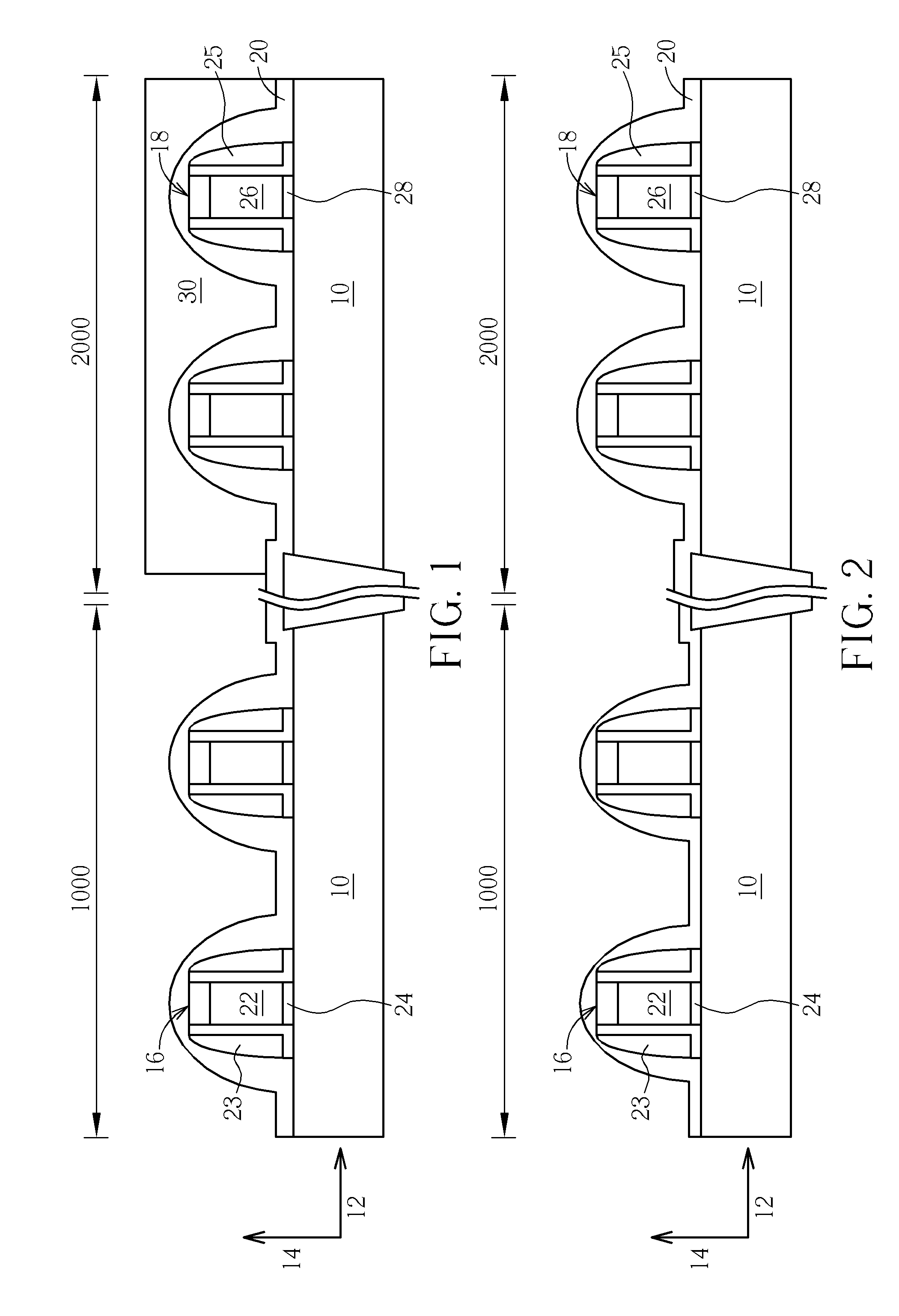
[0022]FIG. 6 to FIG. 9 are schematic cross-sectional diagrams illustrating a method of manufacturing a strained silicon structure in accordance with the present invention, wherein like numerals designate similar or the same parts, regions or elements. The difference between the first preferred embodiment and the second preferred embodiment is that the recess of the first transistor is formed prior to the recess of the second transistor in the second preferred embodiment. The fabricating method of the recess of the first transistor in the second preferred embodiment is the same as that of the first preferred embodiment.

[0023]The method of forming the recess of the first transistor will be described briefly as below. As shown in FIG. 6, a substrate 10 defined into a low density region 1000 and a high density region 2000 is provided. A horizontal direction 12 is parallel to the top substrate of the substrate 10. A vertical direction 14 is perpendicular to the top surface of the substra...


PUM


Abstract

A strained silicon substrate structure includes a first transistor and a second transistor disposed on a substrate. The first transistor includes a first gate structure and two first source / drain regions disposed at two sides of the first gate structure. A first source / drain to gate distance is between each first source / drain region and the first gate structure. The second transistor includes a second gate structure and two source / drain doped regions disposed at two side of the second gate structure. A second source / drain to gate distance is between each second source / drain region and the second gate structure. The first source / drain to gate distance is smaller than the second source / drain to gate distance.

Description

BACKGROUND OF THE INVENTION[0001]1. Field of the Invention[0002]The present invention relates to a strained silicon structure, and more particularly to a strained silicon structure having different channel strain in the high density region and in the low density region.[0003]2. Description of the Prior Art[0004]The performance of Si semiconductor elements, MOSFETs in particular, has increased year after year with the advance of large-scale integrated circuits (LSI). Recently, however, it has appeared that the miniaturization attained by lithographic technology has reached its limit, and that carrier mobility has almost reached theoretical mobility in Si. To attain higher performance of the semiconductor device, attempts have been made to use a strained silicon (Si) layer grown epitaxially on a Si wafer with a silicon germanium (SiGe) layer in a recess in the substrate.[0005]Generally, the wafer can be separated into a high density region and a low density region. The high density re...

Claims


Application Information

Patent Timeline
IPC IPC(8): H01L27/088
CPCH01L21/823807H01L21/823814H01L27/088H01L29/66636H01L29/7848H01L29/165
Inventor HWANG, GUANG-YAWCHOU, LING-CHUNWANG, I-CHANGHUANG, SHIN-CHUANLIAO, JIUNN-HSIUNGCHEN, SHIN-CHILIN, PAU-CHUNGYEH, CHIU-HSIENCHIEN, CHIN-CHENGCHEN, CHIEH-TE
Owner MARLIN SEMICON LTD
Why Eureka
Try Eureka