
Antenna structure

a technology of nanotubes and antennae, applied in the field of nanotube structures, can solve the problems of obstructing the reduction of etc., and achieve the effects of saving occupation space, reducing the size of the portable communication device, and saving research and development costs

Inactive Publication Date: 2012-05-31
INVENTEC CORP
View PDF3 Cites 67 Cited by
  • Summary
  • Abstract
  • Description
  • Claims
  • Application Information

AI Technical Summary

Benefits of technology

[0011]The antenna structure of the present invention can be applied as a near field communication antenna, a radio frequency identification antenna, etc. the antenna structure can be immediately used with a conventional circuit element. Therefore, a research and development cost is saved. Moreover, with this configuration, forming the antenna structure in the non-display area of the display panel especially when the non-display area surrounds the display area of the display panel can save the occupation space in the portable communication device and can effectively reduce the size of the portable communication device.
[0012]Due to the fact that the coil unit can be formed on the same layer with the signal line or the scanning line of the display panel when the antenna structure is manufactured, a conventional ITO film for forming the signal line or the scanning line is used as the conductive film for forming the coil unit. This not only simplifies a manufacturing process, but also effectively thins the display panel.
[0013]If the antenna structure of the present invention is applied to the touch-control display panel, which is the same as the above antenna structure formed on a general display panel, the coil unit can be formed on the same layer with the X-axis touch-control line or the Y-axis touch-control line of the touch-control display panel. This not only simplifies the manufacturing process, but also effectively thins the touch-control display panel due to the fact that the coil unit can be formed on the same layer with the X-axis touch-control line or the Y-axis touch-control line.
[0014]The electrodes can be made of flexible circuit boards or can be probe-type electrodes. When the electrodes are made of the flexible circuit boards, positions of the display panel and a circuit board of the portable communication device, etc. can be flexibly designed and arranged, and the antenna structure is electrically connected with the circuit boards through the electrodes made of the flexible circuit boards. When the electrodes are the probe-type electrodes, wireless signals received by the antenna structure can be transmitted by the low-impedance probe-type electrodes with low leakage.
[0015]Moreover, the antenna structure of the present invention can further include a shielding layer covering the coil unit. The shielding layer inhibits a noise and improves the quality of transmitting the wireless signals.

Problems solved by technology

For a function of receiving and transmitting the signals, the above induction coil needs to have a larger induction range, thus occupying a space in the portable communication device and obstructing the reduction of the size of the portable communication device.
Therefore, a research and development cost is saved.

Method used


Image

  • Antenna structure
  • Antenna structure
  • Antenna structure

Examples


Embodiment Construction

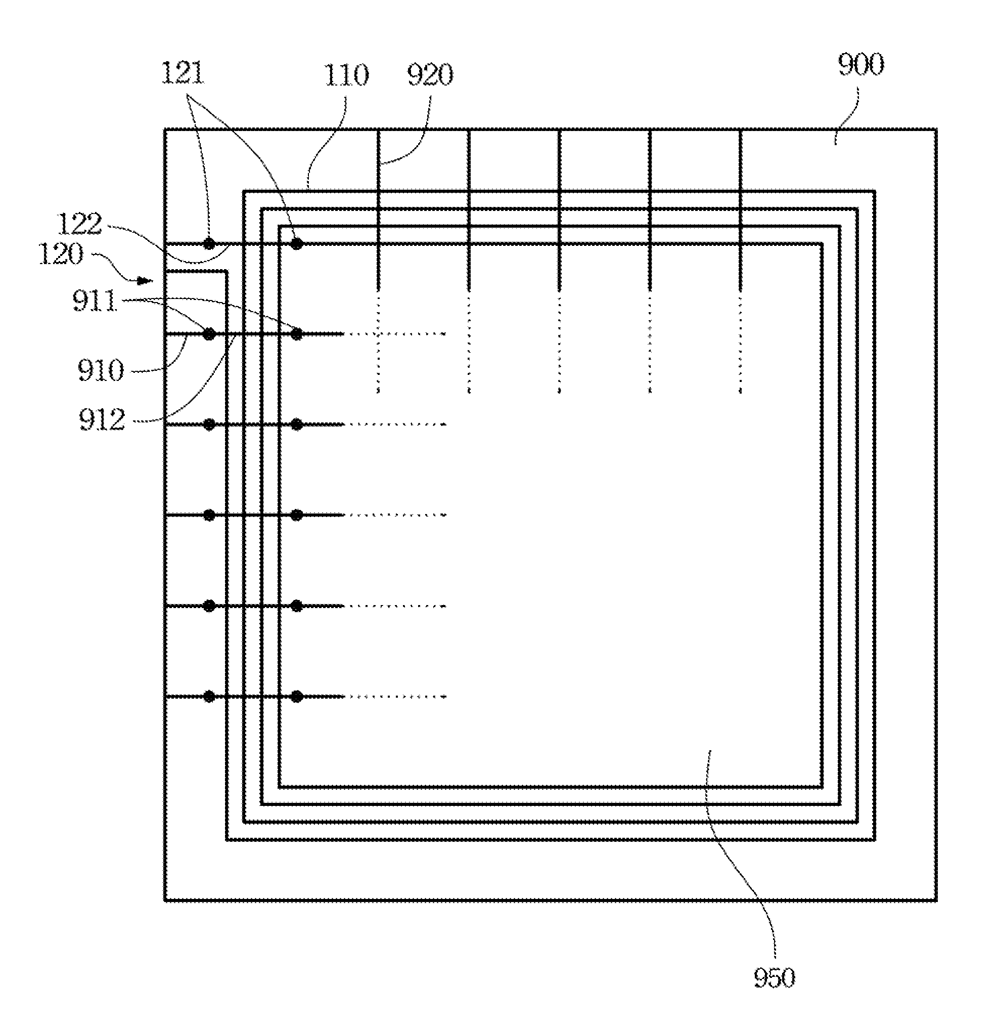
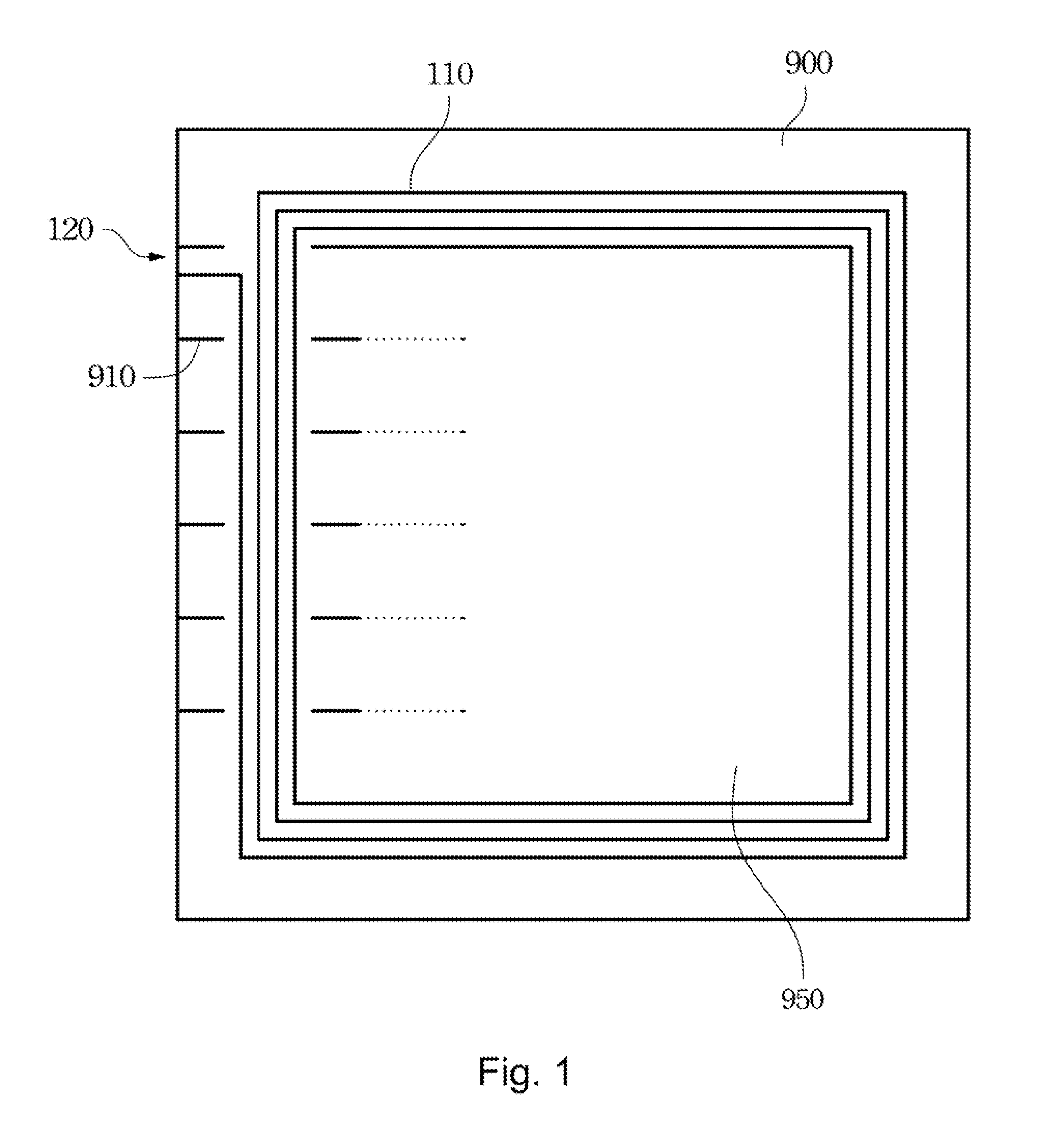
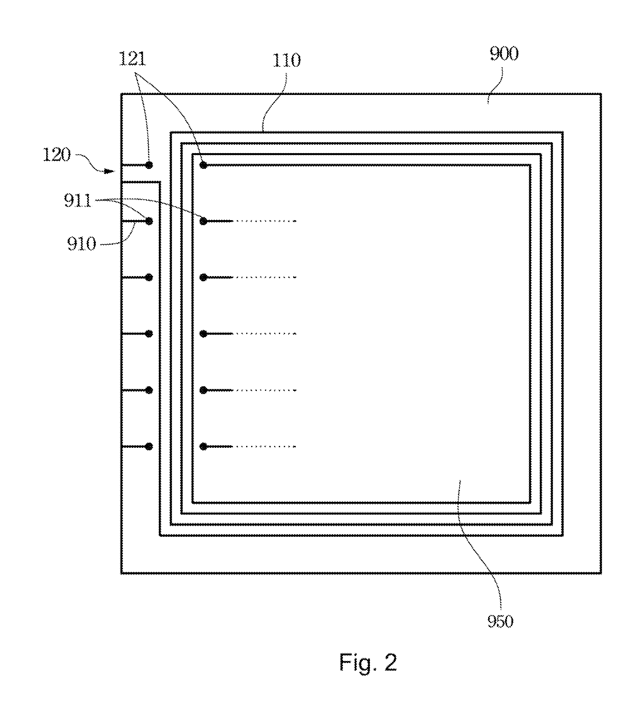
[0021]The antenna structure of the present invention includes a coil unit 110 and electrodes 120. The coil unit 110 is formed in a non-display area of a display panel 900 by etching a conductive film on the display panel 900. The non-display area shown in the figures surrounds a display area 950 of the display panel 900, but the present invention is not limited to this. For example, the non-display area may also be located at any position, such as above the display area 950, below the display area 950, on the left of the display area 950, or on the right of the display area 950. The above conductive film can be a conductive film made of the same material as that of a signal line or a scanning line of the display panel 900, e.g. an ITO film. The electrodes 120 are located at terminals of the coil unit 110 and electronically connected to the coil unit 110 and a circuit board of a portable communication device equipped with the antenna structure (e.g. a mobile phone or a personal digit...


PUM


Abstract

An antenna structure includes a coil unit formed by etching a conductive film in a non-display area of a display and a set of electrodes for transmitting signals connected to terminals of the coil unit. The antenna structure can be a near field communication antenna or a radio frequency identification antenna to transmit and receive signals with the coil unit formed in the non-display area of the display to save the occupation space in a portable communication device. Therefore, the antenna structure can effectively reduce the size of the portable communication device.

Description

RELATED APPLICATIONS[0001]This application claims priority to Taiwan Application Serial Number 099141509, filed Nov. 30, 2010, which is herein incorporated by reference.BACKGROUND[0002]1. Field of Invention[0003]The present invention relates to an antenna structure, and more particularly, to an antenna structure formed on a display panel.[0004]2. Description of Related Art[0005]An antenna for receiving and transmitting signals is disposed in a portable communication device, e.g. an antenna for near field communication (NFC) or radio frequency identification (RFID). A current antenna structure is manufactured by winding a wire such as an enamel-covered wire into an induction coil, encapsulating the above induction coil with an insulating film and then disposing it within the portable communication device, or by directly making the wire such as the enamel-covered wire surround an interior of a case of the portable communication device to form the induction coil. A tap of the induction...

Claims


Application Information

Patent Timeline
IPC IPC(8): G06F3/041C30B33/08H01Q1/22
CPCG06F3/044H01Q7/00H01Q1/38H01Q1/2225G06F3/0443G06F3/0446
Inventor CHEN, CHIH-JUNG
Owner INVENTEC CORP
Features
  • Generate Ideas
  • Intellectual Property
  • Life Sciences
  • Materials
  • Tech Scout
  • Unparalleled Data Quality
  • Higher Quality Content
  • 60% Fewer Hallucinations
Learn More