Storage nodes, magnetic memory devices, and methods of manufacturing the same

a technology of magnetic memory and storage nodes, applied in the field of memory devices, can solve problems such as affecting the integration of magnetic memory devices, and achieve the effect of reducing standby power

Active Publication Date: 2012-06-07
SAMSUNG ELECTRONICS CO LTD
View PDF1 Cites 17 Cited by
  • Summary
  • Abstract
  • Description
  • Claims
  • Application Information

AI Technical Summary

Benefits of technology

[0049]By using magnetic memory devices according to one or more example embodiments, a magnetic DRAM as a next gen

Problems solved by technology

Considering the relatively high integration of memory devices, requiring a separate wiring for g

Method used


Image

  • Storage nodes, magnetic memory devices, and methods of manufacturing the same
  • Storage nodes, magnetic memory devices, and methods of manufacturing the same
  • Storage nodes, magnetic memory devices, and methods of manufacturing the same

Examples


Embodiment Construction

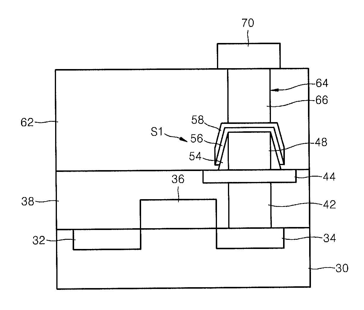
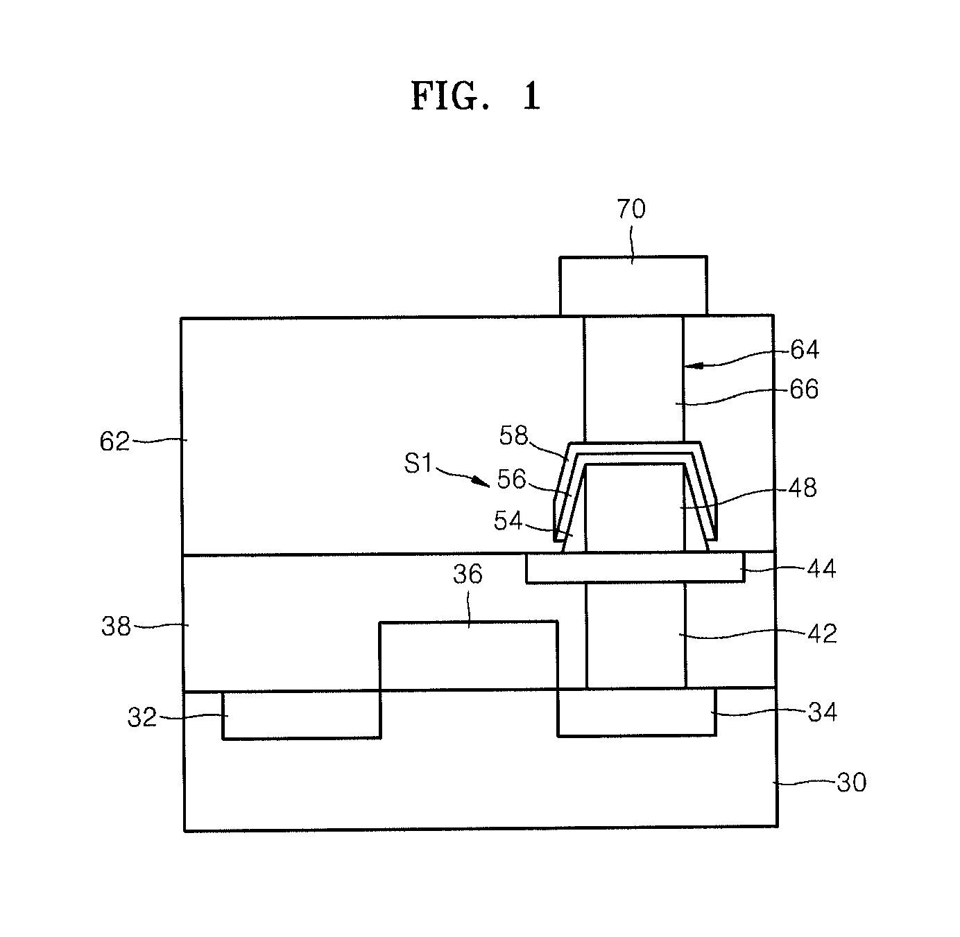
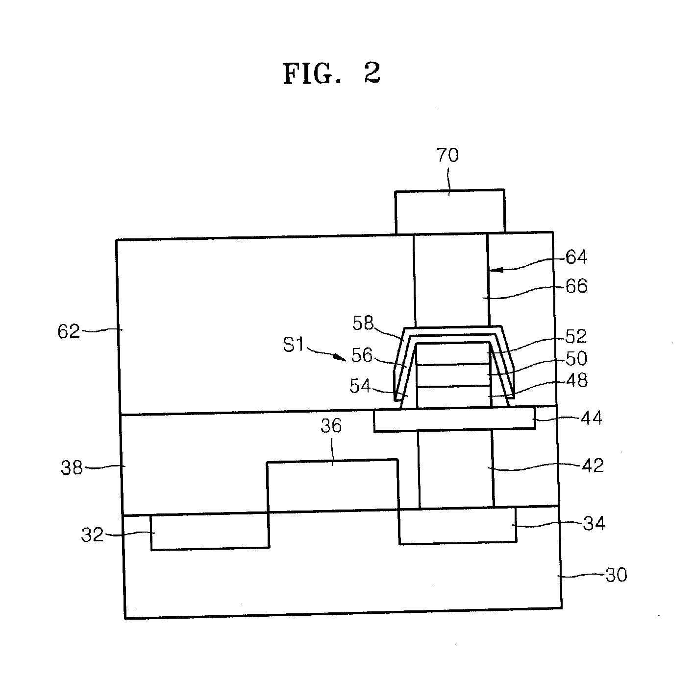
[0067]Example embodiments will now be described more fully with reference to the accompanying drawings, in which some example embodiments are shown. In the drawings, the thicknesses of layers and regions are exaggerated for clarity. Like reference numerals in the drawings denote like elements.

[0068]Detailed illustrative embodiments are disclosed herein. However, specific structural and functional details disclosed herein are merely representative for purposes of describing example embodiments. Example embodiments may be embodied in many alternate forms and should not be construed as limited to only those set forth herein.

[0069]It should be understood, however, that there is no intent to limit this disclosure to the particular example embodiments disclosed. On the contrary, example embodiments are to cover all modifications, equivalents, and alternatives falling within the scope of the invention. Like numbers refer to like elements throughout the description of the figures.

[0070]It w...


PUM


Abstract

A storage node of a magnetic memory device includes: a lower magnetic layer, a tunnel barrier layer formed on the lower magnetic layer, and a free magnetic layer formed on the tunnel barrier. The free magnetic layer has a magnetization direction that is switchable in response to a spin current. The free magnetic layer has a cap structure surrounding at least one material layer on which the free magnetic layer is formed.

Description

CROSS-REFERENCE TO RELATED APPLICATIONS[0001]This application claims priority under 35 U.S.C. §119 to Korean Patent Application No. 10-2010-0124440, filed on Dec. 7, 2010, in the Korean Intellectual Property Office, and Korean Patent Application No. 10-2011-0107058, filed on Oct. 19, 2011, in the Korean Intellectual Property Office, the disclosures of which are incorporated herein in their entirety by reference.BACKGROUND[0002]1. Field[0003]Example embodiments relate to memory devices, for example, storage nodes including a free magnetic layer of a magnetic anisotropy material, magnetic memory devices including storage nodes, and / or methods of manufacturing storage nodes and magnetic memory devices including storage nodes.[0004]2. Description of the Related Art[0005]In the field of magnetic tunnel junctions (MTJs), a magnetic random access memory (MRAM) having a tunneling magnetoresistance (TMR) effect has been researched as a next generation non-volatile memory device due to its no...

Claims


Application Information

Patent Timeline
IPC IPC(8): H01L29/82H01L21/04
CPCH01L27/228H01L29/82G11C11/161H01L43/12H01L43/08H10B61/22H10N50/10H10N50/01
Inventor KIM, KWANG-SEOKCHUNG, U-INSHIN, JAI-KWANGKIM, KEE-WONLEE, SUNG-CHULPI, UNG-HWAN
Owner SAMSUNG ELECTRONICS CO LTD
Why Eureka
Try Eureka